 | –≠–ª–µ–∫—Ç—Ä–æ–Ω–Ω—ã–π –∫–æ–º–ø–æ–Ω–µ–Ω—Ç: HAL740 | –°–∫–∞—á–∞—Ç—å:  PDF PDF  ZIP ZIP |

HAL700, HAL740
Hall-Effect Sensors
with Independent Outputs
Edition June 13, 2002
6251-477-1DS
DATA SHEET
MICRONAS
MICRONAS

HAL700, HAL740
DATA SHEET
2
June 13, 2002; 6251-477-1DS
Micronas
Contents
Page
Section
Title
3
1.
Introduction
3
1.1.
Features
3
1.2.
Family Overview
4
1.3.
Marking Code
4
1.3.1.
Special Marking of Prototype Parts
4
1.4.
Operating Junction Temperature Range
4
1.5.
Hall Sensor Package Codes
4
1.6.
Solderability
5
2.
Functional Description
8
3.
Specifications
8
3.1.
Outline Dimensions
8
3.2.
Dimensions of Sensitive Areas
8
3.3.
Positions of Sensitive Areas
9
3.4.
Absolute Maximum Ratings
9
3.4.1.
Storage, Moisture Sensitivity Class, and Shelf Life
9
3.5.
Recommended Operating Conditions
10
3.6.
Electrical Characteristics
14
4.
Type Description
14
4.1.
HAL700
16
4.2.
HAL740
18
5.
Application
18
5.1.
Ambient Temperature
18
5.2.
Extended Operating Conditions
18
5.3.
Start-up Behavior
18
5.4.
EMC and ESD
20
6.
Data Sheet History

DATA SHEET
HAL700, HAL740
Micronas
June 13, 2002; 6251-477-1DS
3
Dual Hall-Effect Sensors with Independent Outputs
1. Introduction
The HAL700 and the HAL740 are monolithic CMOS
Hall-effect sensors consisting of two independent
switches controlling two independent open-drain out-
puts. The Hall plates of the two switches are spaced
2.35 mm apart.
The devices include temperature compensation and
active offset compensation. These features provide
excellent stability and matching of the switching points
in the presence of mechanical stress over the whole
temperature and supply voltage range.
The sensors are designed for industrial and automo-
tive applications and operate with supply voltages
from 3.8 V to 24 V in the ambient temperature range
from
-
40
∞
C up to 125
∞
C.
The HAL700 and the HAL740 are available in the
SMD package SOT-89B.
1.1. Features
≠ two independent Hall-switches
≠ distance of Hall plates: 2.35 mm
≠ switching offset compensation at typically 150 kHz
≠ operation from 3.8 V to 24 V supply voltage
≠ operation with static and dynamic magnetic fields up
to 10 kHz
≠ overvoltage protection at all pins
≠ reverse-voltage protection at V
DD
-pin
≠ robustness of magnetic characteristics against
mechanical stress
≠ short-circuit protected open-drain outputs
by thermal shut down
≠ constant switching points over a wide
supply voltage range
≠ EMC corresponding to DIN 40839
1.2. Family Overview
The types differ according to the switching behavior of
the magnetic switching points at the both Hall plates
S1 and S2.
Latching Sensors:
The output turns low with the magnetic south pole on
the branded side of the package. The output maintains
its previous state if the magnetic field is removed. For
changing the output state, the opposite magnetic field
polarity must be applied.
Unipolar Sensors:
In case of a south-sensitive switch, the output turns
low with the magnetic south pole on the branded side
of the package and turns high if the magnetic field is
removed. The switch does not respond to the mag-
netic north pole on the branded side.
In case of a north-sensitive switch, the output turns low
with the magnetic north pole on the branded side of
the package and turns high if the magnetic field is
removed. The switch does not respond to the mag-
netic south pole on the branded side.
Type
Switching Behavior
See
Page
HAL700
S1: latching
S2: latching
14
HAL740
S1: unipolar north sensitive
S2: unipolar south sensitive
16
HAL700, HAL740
DATA SHEET
4
June 13, 2002; 6251-477-1DS
Micronas
1.3. Marking Code
All Hall sensors have a marking on the package sur-
face (branded side). This marking includes the name
of the sensor and the temperature range.
1.3.1. Special Marking of Prototype Parts
Prototype parts are coded with an underscore beneath
the temperature range letter on each IC. They may be
used for lab experiments and design-ins but are not
intended to be used for qualification tests or as produc-
tion parts.
1.4. Operating Junction Temperature Range
The Hall sensors from Micronas are specified to the
chip temperature (junction temperature T
J
).
K: T
J
=
-
40
∞
C to +140
∞
C
E: T
J
=
-
40
∞
C to +100
∞
C
The relationship between ambient temperature (T
A
)
and junction temperature is explained in Section 5.1.
on page 18.
1.5. Hall Sensor Package Codes
Hall sensors are available in a wide variety of packag-
ing quantities. For more detailed information, please
refer to the brochure: "Hall Sensors: Ordering Codes,
Packaging, Handling".
1.6. Solderability
All packages: according to IEC68-2-58
During soldering, reflow processing and manual
reworking, a component body temperature of 260
∞
C
should not be exceeded.
Components stored in the original packaging should
provide a shelf life of at least 12 months, starting from
the date code printed on the labels, even in environ-
ments as extreme as 40
∞
C and 90% relative humidity.
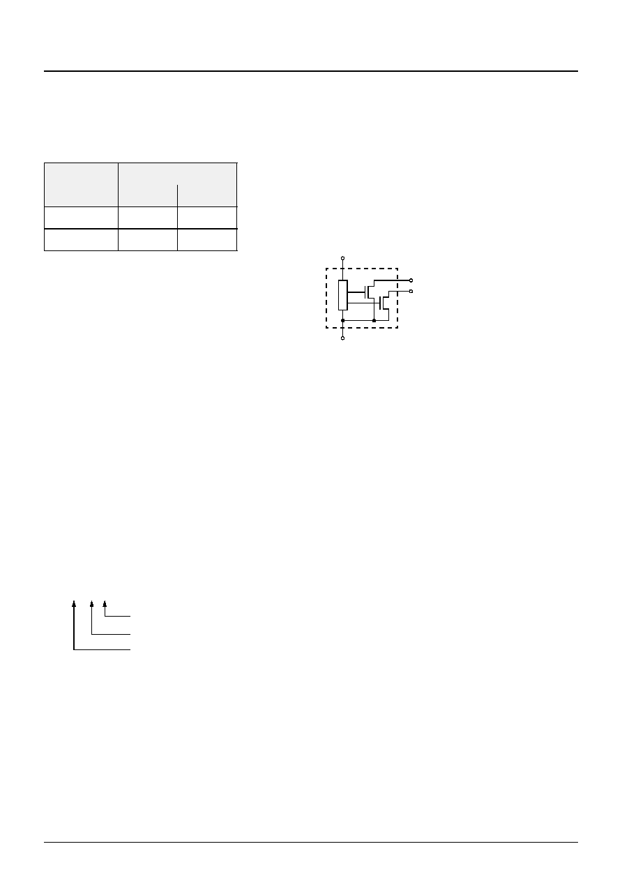
Fig. 1≠1: Pin configuration
Type
Temperature Range
K
E
HAL700
700K
700E
HAL740
740K
740E
HALXXXPA-T
Temperature Range: K or E
Package: SF for SOT-89B
Type: 700
Example: HAL700SF-K
Type: 700
Package: SOT-89B
Temperature Range: T
J
=
-
40
∞
C to +140
∞
C
1 V
DD
4
GND
3 S1-Output
2 S2-Output
DATA SHEET
HAL700, HAL740
Micronas
June 13, 2002; 6251-477-1DS
5
2. Functional Description
The HAL700 and the HAL740 are monolithic inte-
grated circuits with two independent subblocks each
consisting of a Hall plate and the corresponding com-
parator. Each subblock independently switches the
comparator output in response to the magnetic field at
the location of the corresponding sensitive area. If a
magnetic field with flux lines perpendicular to the sen-
sitive area is present, the biased Hall plate generates a
Hall voltage proportional to this field. The Hall voltage
is compared with the actual threshold level in the com-
parator. The subblocks are designed to have closely
matched switching points. The output of comparator 1
attached to S1 controls the open drain output at Pin 3.
Pin 2 is set according to the state of comparator 2 con-
nected to S2.
The temperature-dependent bias ≠ common to both
subblocks ≠ increases the supply voltage of the Hall
plates and adjusts the switching points to the decreas-
ing induction of magnets at higher temperatures. If the
magnetic field exceeds the threshold levels, the com-
parator switches to the appropriate state. The built-in
hysteresis prevents oscillations of the outputs.
The magnetic offset caused by mechanical stress is
compensated for by use of "switching offset compen-
sation techniques". Therefore, an internal oscillator
provides a two-phase clock to both subblocks. For
each subblock, the Hall voltage is sampled at the end
of the first phase. At the end of the second phase, both
sampled and actual Hall voltages are averaged and
compared with the actual switching point.
Shunt protection devices clamp voltage peaks at the
output pins and V
DD
-pin together with external series
resistors. Reverse current is limited at the V
DD
-pin by
an internal series resistor up to
-
15 V. No external
reverse protection diode is needed at the V
DD
-pin for
reverse voltages ranging from 0 V to
-
15 V.
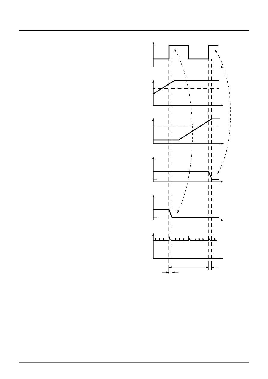
Fig. 2≠2 and Fig. 2≠3 on page 6 show how the output
signals are generated by the HAL700 and the
HAL740. The magnetic flux density at the locations of
the two Hall plates is shown by the two sinusodial
curves at the top of each diagram. The magnetic
switching points are depicted as dashed lines for each
Hall plate separately.
Fig. 2≠1: HAL700 timing diagram with respect to the
clock phase
t
Clock
t
BS1
t
BS2
t
Pin 2
t
Pin 3
t
I
DD
BS1
on
BS2
on
V
OH
V
OL
V
OH
V
OL
1/f
osc
t
f
t
f