 | –≠–ª–µ–∫—Ç—Ä–æ–Ω–Ω—ã–π –∫–æ–º–ø–æ–Ω–µ–Ω—Ç: OPT0256C | –°–∫–∞—á–∞—Ç—å:  PDF PDF  ZIP ZIP |

OPT 0256C
Photo Detector Array IC
Edition May 15, 2002
6251-581-1AI
ADVANCE INFORMATION
MICRONAS

OPT 0256C
ADVANCE INFORMATION
2
May 15, 2002; 6251-581-1AI
Micronas
Contents
Page
Section
Title
3
1.
Introduction
4
2.
Functional Description
4
2.1.
Photodiode
4
2.2.
Analog-to-Digital Converter
4
2.2.1.
Current Offset
4
2.3.
Accumulation Counter
5
2.4.
Control Logic and Serial Interface
6
2.4.1.
Commands
7
2.4.1.1.
ACCUCTR
7
2.4.1.2.
GAIN_WR
7
2.4.1.3.
RESET
7
2.4.1.4.
DRIVER
7
2.4.1.5.
START
7
2.4.1.6.
STOP
7
2.4.1.7.
DUMMY
7
2.4.1.8.
IRQ_ACKN
7
2.4.1.9.
READ D_RD_ .. FIRST, NEXT, TERM
8
2.4.1.10.
T_RD_FIRST, T_RD_LAST
8
2.4.1.11.
MODE CONT
9
2.4.1.12.
MODE EXT_START
9
2.4.1.13.
MODE EXT_START_STOP
9
2.4.1.14.
MODE HOLD
9
2.5.
Temperature Sensor
9
2.6.
Biasing and Reference Circuit
9
2.7.
Voltage Regulator for Counter/Shifter Cells
11
2.8.
Current Adder
12
3.
Specifications
12
3.1.
Package for Evaluation Purposes
12
3.2.
Outline Dimensions (Preliminary)
13
3.3.
Pin Connections and Short Descriptions
14
3.4.
Pin Descriptions
15
3.5.
Pin Configuration
16
3.6.
Pin Circuits
17
3.7.
Characteristics
17
3.7.1.
Absolute Maximum Ratings
17
3.7.2.
Recommended Operating Conditions
18
3.7.3.
Electrical Characteristics
19
3.7.4.
Geometrical Characteristics
20
3.7.5.
Optical and Electro-optical Characteristics
21
3.7.6.
UV Degradation
22
4.
Application Notes
22
4.1.
Data Read Out
22
4.2.
Blocking Capacitors
22
4.3.
Cascading
24
5.
Data Sheet History

ADVANCE INFORMATION
OPT 0256C
Micronas
May 15, 2002; 6251-581-1AI
3
Photo Detector Array IC
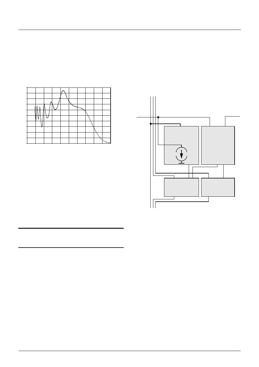
1. Introduction
The OPT 0256C is a 256-channel PDA (photo detector
array) IC with all-digital I/O.
The PDA consists of 256 photodiodes each having its
own 16-bit ADC, an analog biasing circuit with inte-
grated bandgap voltage reference, a settable accumu-
lation counter for wide accumulation range, a tempera-
ture sensor with ADC and a digital control block with
Motorola SPI-compatible serial interface.
The IC is manufactured in a standard CMOS process
with some additional steps for defining the broad spec-
tral range photodiodes.
Fig. 1≠1 shows a functional block diagram of the
OPT 0256C PDA IC. Test circuitry is not shown.
Four different operation modes are possible:
≠ Continuous Mode
≠ External Start Mode
≠ External Start/stop Mode
≠ Hold Mode
Fig. 1≠1: OPT 0256C PDA block diagram
Photodiode
ADC
Shift Register
ADC
Shift Register
Temperature
Sensor
Photodiode
ADC
Shift Register
Photodiode
ADC
Shift Register
Biasing and
Reference
Circuit
Accumulation
Counter
Accumulation Counter
for Temperature Sens.
0
1
254
255
.
.
.
.
.
.
.
.
.
.
.
.
Photodiode
ADC
Shift Register
Control Logic
and
Serial Interface
gain
SC
L
K
MO
S
I
MIS
O
PC
SE
N
Q
DA
V
Q
RE
S
E
TQ
MC
L
K
ST
AR
T
_
A
C
Voltage Regulator
for Counter/Shifter
Cells
VD
D
AV
D
D
SV
D
D
ADC
Clock
Generator
OPT 0256C
ADVANCE INFORMATION
4
May 15, 2002; 6251-581-1AI
Micronas
2. Functional Description
2.1. Photodiode
A reverse-biased PN junction serves as a photodiode.
A special diode construction provides a broad spectral
sensitivity from UV to IR and hardness against UV irra-
diation.
Fig. 2≠1: Photodiode quantum efficiency
2.2. Analog-to-Digital Converter
A first-order
-
converter is used. A digital counter
serves as a simple decimation filter. It accumulates the
number of pulses provided by the ADC every accumu-
lation cycle.
Accumulation cycle time interval information and read
out is controlled by the controlling block and pro-
gramed via the SPI interface.
Note: Counter overflows can occur for accumulation
counter values >2
16
-
2. After an overflow, the
counter will be stopped.
2.2.1. Current Offset
A current adder is integrated for test purposes, i.e. to
test some functionality without optical stimulation. It
can also be used to determine the relative gain factors
for each channel for different gain selections.
For normal operation, the current adder is switched off.
Operation of the current adder is described in section
(see Section 2.8. on page 11).
Fig. 2≠2: ADC block diagram
2.3. Accumulation Counter
The length of the time interval for sampling is deter-
mined by a 26-bit down-counter with zero detection.
The accumulation time results in:
(ACCUCTR+1)
◊
f
MCLK
.
With 5 MHz count frequency, the maximum accumula-
tion interval time is 2
26
◊
200 ns=13.4 s, with
ACCUCTR=2
26
-
1.The load value, start and stop are
programmed with the SPI interface. In normal applica-
tion mode the accumulation counter has a continuous
load, it is not necessary to refresh the time interval.The
start stop is also possible with a signal edge at the pin
START_ACQ.
The accumulation counter load register value is not
affected by MODE commands. The reset value of the
counter is 2
16
-
2 (000FFFE hex).
0.000
0.100
0.200
0.300
0.400
0.500
0.600
0.700
0.800
0.900
1.000
100
200
300
400
500
600
700
800
900
1000
1100
Wavelength [nm]
QE
from
photo-
diode
Current Adder
Gain
Shift Register
Current Adder
Shift Register
to ADC
and ADC disable
ADC
analog part
digital
part
ADVANCE INFORMATION
OPT 0256C
Micronas
May 15, 2002; 6251-581-1AI
5
2.4. Control Logic and Serial Interface
For programming the PDA and for communication with
the controller or signal processor, a standard SPI inter-
face is used.
It is a 4-wire interface driven by master (controller or
signal processor) with following features:
≠ Input MOSI driven by master
≠ Serial clock SCLK driven by master
≠ Chip select PCSENQ driven by master
≠ Output MISO driven by slave
≠ Input data on MOSI is latched with positive edge of
SCLK
≠ Max. clock frequency is 5.5 MHz, static design
≠ Word length is (n
◊
8 bit) with 4-bit command MSB
first and (4 + (n
-
1)
◊
8) bit data MSB first.
≠ Between two commands, the PCSENQ must go
high for at least two clock cycles (end of command
detection)
Output MISO of PDA is high-impedance in reset or
when PCSENQ is high. In active mode MISO is only in
low impedance during read data cycles.
When the accumulation counter detects zero or any
other STOP signal occurs, DAVQ (DATA available
interrupt signal to master) will be active. DAVQ can be
reset by commands described later.
Different modes which control the accumulation time
are possible. Selection of a mode is done with the
MODE command and the four following data bits.
The different READ commands need also the four fol-
lowing data bits to determine the appropriate com-
mand.
The external START_ACQ signal is an asynchronous
signal. It has an internal delay of max. 2 clock cycles to
start or stop the accumulation counter.
Cascading of PDAs or multi-user SPI is possible.
Then, the PCSENQ must be individually addressed.
Fig. 2≠3: SPI interface timing
SCLK
MOSI
instruction bits
mode / data bits
MSB
PCSENQ
MISO
Answer after Command
x
z
x
40 ns < x < T
SCLK_LOW
0 <= z < T
SCLK_LOW
Data request (D_RD_FIRST, D_RD_NEXT, T_RD_FIRST, T_RD_LAST)
MSB
hiZ
hiZ

OPT 0256C
ADVANCE INFORMATION
6
May 15, 2002; 6251-581-1AI
Micronas
2.4.1. Commands
Table 2≠1: SPI Interface Commands
Code
Command
Description
0110
ACCUCTR
Shifts (serial data length
-
4) data bits into the accumulation counter load register.
1110
GAIN_WR
p
◊
2-bit gain values for each channel, p=(serial data frame length
-
4)/2.
1001
RESET
Sets all registers and counters into RESET state.
0101
DRIVER
Sets the MISO output driving capability (bits 4...7).
1000
START
Enables accumulation counter (decoded after 4 SCLK cycles).
0100
STOP
Disables accumulation counter (decoded after 4 SCLK cycles).
1100
DUMMY
No output change is produced at the next command. This command is used to
get the counter/shifter value of the last channel or as continue command for 8 bit
command length.
1101
IRQ_ACKN
Clears DAVQ.
0001
010
MODE
CONT
Continuous mode. Switches accumulation counter in autoload mode, clears
DAVQ signal once, resets counter/shifter cells.
0001
001
MODE
EXT_START
External start mode. Loads accumulation counter, clears DAVQ signal once,
resets counter/shifter cells.
0001
111
MODE
EXT_START_ STOP
External start/stop mode. Resets counter/shifter cells, disables accumulation
counter and switches the commands START/STOP and the external signal
START_ACQ directly to the counter enable signal, clears DAVQ signal once
0001
011
MODE
HOLD
Hold mode. Disables accumulation counter, disables counter/shifter. DAVQ and
MISO stay in their previous state.
1111
010
READ
D_RD_FIRST
Clears DAVQ signal, starts shift clock, sets first counter in shift mode.
1111
111
READ
D_RD_NEXT
Sets next counter/shifter cell in shift mode.
1111
011
READ
D_RD_TERM
Terminates the READ D_RD_NEXT command cycle. Resets the internal read-
out pointer. The MISO output buffer is set to high impedance state for command
lengths > 16. For 8-bit command lengths, MISO is set to high-impedance after
the following command.
1111
101
READ
T_RD_FIRST
Sets counter/shifter cell of the temperature sensor into shift mode, enables the
output of the temperature sensor channels.
1111
110
READ
T_RD_LAST
Sets counter/shifter cell of the temperature sensor into count mode, disables the
output of the temperature sensor channels.
1011
FLAGS
Data bit 0 ENCURADD: Enables (1) / disables (0) all current adders (reset val.:
0).
Data bit 1 FLATRES: Disables (1) / enables (0) "flat response" (reset val.: 0).
0111
BRANCH_WR
p
◊
3-bit branch selection values for each channel in case of "flat response" dis-
abled, p=(serial data frame length
-
4)/3.
1010
ADCUR_WR
p
◊
8-bit current adder/ADC disable values for each channel, p=(serial data frame
length
-
4)/8.

ADVANCE INFORMATION
OPT 0256C
Micronas
May 15, 2002; 6251-581-1AI
7
2.4.1.1. ACCUCTR
The data bits of each ACCUCTR command are shifted
in the accumulation counter load register. Data is
aligned MSB first. To load the complete 26 bit register,
i.e. three 16-bit ACCUCTR commands are necessary.
In this case the 10 MSB of the 36-bit data word are
lost.
2.4.1.2. GAIN_WR
The gain value for each channel can be separately
selected. A 256x2 bit shift register chain can be loaded
with the appropriate values. This can be done via the
GAIN_WR command. This command writes gain val-
ues for n/2 channels, where n is the number of data
bits in the serial data word. Gain data is aligned MSB
of first channel first. The gain data is written in the last
channel, all data bits in the gain shift register are
shifted towards the first channel. Gain data of the n/2
first channels is lost after each GAIN_WR command.
After reset, the gain value is set to 2.
2.4.1.3. RESET
RESET is an equivalent to a hardware reset via the
RESETQ pin. Counter/shifter cells are cleared,
ACCUCTR is set to 2
16
-
2, DRIVER is set to 0 (weak-
est), MODE HOLD is selected.
2.4.1.4. DRIVER
The first 4 data bits (MSB first) select the MISO output
buffer driving capability. Therefore, a linear 4-bit DAC
with offset is used. The DRIVER value depends on the
desired rise and fall times and on the load impedance.
To minimize interferences, the rise and fall times
should be as long as possible. Therefore, the DRIVER
value should be a minimum.
2.4.1.5. START
Start of accumulation cycle. Necessary in all modes.
In MODE CONT, this command starts the accumula-
tion cycle for the first time, no further START com-
mands are necessary.
A falling edge of the hardware signal START_ACQ is
equivalent to the START command.
2.4.1.6. STOP
End of accumulation cycle in MODE:
EXT_START_STOP.
A rising edge of the hardware signal START_ACQ is
equivalent to the STOP command.
2.4.1.7. DUMMY
This command is used to add additional bits to 8-bit
commands to read out 16 bit data. No internal states
are changed.
2.4.1.8. IRQ_ACKN
This command clears the DAVQ signal. No other inter-
nal states are changed. The READ D_RD_FIRST
command clears the DAVQ signal, too.
2.4.1.9. READ D_RD_ .. FIRST, NEXT, TERM
The READ D_RD_FIRST command selects the first
channel to be read out with the following command
and activates the MISO output buffer.
The READ D_RD_NEXT command selects the next
channel to be read out with the following command.
The READ D_RD_TERM command terminates the
readout cycle and sets the MISO output buffer to high-
impedance state with the following positive edge of
PCSENQ. In the case of 8-bit commands, the MISO
output buffer goes to high-impedance state after the
READ D_RD_TERM following DUMMY command.
A complete readout command sequence looks like the
following list:
≠ READ D_RD_FIRST: select the first channel for
data readout.
≠ READ D_RD_NEXT:
select the 2
nd
channel for
data readout while reading
out first channel data.
≠ READ D_RD_NEXT:
select the 3
rd
channel for
data readout while reading
out 2
nd
channel data.
≠ ...
≠ READ D_RD_NEXT:
select the last channel for
data readout while reading
out data of the last but one
channel.
≠ READ D_RD_TERM: prepare termination of the
readout cycle at the next
rising PCSENQ edge while
reading out data of the last
channel.

OPT 0256C
ADVANCE INFORMATION
8
May 15, 2002; 6251-581-1AI
Micronas
In case of 8-bit commands, the command DUMMY is
necessary after the READ D_RD_FIRST, every READ
D_RD_NEXT and the READ D_RD_TERM command.
The first 8 MSBs of the first channel data is available
with the first READ D_RD_NEXT command, the
8 LSBs are available with the following DUMMY com-
mand.
In the case of command widths of 24-bit or more, the
first 16 data bits are valid, all other data bits are zero.
For continuous data readout, the command READ
D_RD_TERM is not necessary after every 255
th
READ
D_RD_NEXT command. The last channel data is then
read out during the following READ D_READ_FIRST
command.
Note: After detecting the DAVQ signal, the master
must read out all data of the 256 channels
(except for fast readout, see next note), other-
wise the data of the next but one accumulation
cycle will be invalid.
Except for switching modes, there is no explicit
reset of the counter/shifter cells to avoid interfer-
ences. Resetting is done by reading out each
channel.
Note: For fast readout, i.e. to measure fast input tran-
sients with lower resolution, it is possible to read
out only a few of the first channels. The readout
sequence must be terminated by the READ
D_RD_TERM command, otherwise signal colli-
sions on the internal data bus occur.
2.4.1.10. T_RD_FIRST, T_RD_LAST
The data from the temperature sensor can be read
with the next command after T_RD_FIRST. Tempera-
ture reading is possible outside any counter/shifter
data reading block surrounded by D_RD_FIRST and
D_RD_LAST.
T_RD_FIRST switches the MISO output buffer with the
next positive edge of PCSENQ to low-impedance
state, T_RD_LAST switches it back to high-impedance
state with the next positive edge of PCSENQ.
With 8-bit command width, a DUMMY command after
T_RD_FIRST and T_RD_LAST is necessary. Data is
then available while the T_RD_LAST and the following
DUMMY command.
With 16-bit commands there is no additional command
DUMMY necessary, and with longer commands only
the first 16 bits are valid data.
Examples for valid command sequences:
≠ ...
≠ D_RD_TERM: terminate reading of counter/shifter
data
≠ T_RD_FIRST: address temperature sensor
(MISO: HiZ)
≠ [DUMMY: only for 8 bit command length]
≠ T_RD_ LAST: read temperature
≠ [DUMMY: read temperature 8 LSB, only for 8 bit
command length]
≠ D_RD_FIRST:address counter/shifter 0 (MISO: HiZ)
≠ ...
2.4.1.11. MODE CONT
This command loads the accumulation counter with
the accumulation counter load register value, clears
the DAVQ signal, resets the counter/shifter cells and
switches to the continuous mode.
With a START command or a negative edge of the
external signal START_ACQ, down counting of the
accumulation counter is started.
After zero detection,
≠ the accumulation counter will be reloaded automati-
cally,
≠ the counter/shifter cells are switched between
counting and shifting,
≠ down counting of the accumulation counter will be
restarted automatically,
≠ the signal DAVQ is set to low.
This cycle will be repeated endlessly and can not be
stopped with the STOP command or any edge of the
external START_ACQ signal.
Note: To increase resolution and dynamic range, a set
of following readouts can be added or otherwise
decimated. In this case, set ACCUCTR=65534.
ADVANCE INFORMATION
OPT 0256C
Micronas
May 15, 2002; 6251-581-1AI
9
2.4.1.12. MODE EXT_START
This command loads the accumulation counter with
the accumulation counter load register value, clears
the DAVQ signal, resets the counter/shifter cells, and
switches to the external start mode.
With a START command or a negative edge of the
external signal START_ACQ, down-counting of the
accumulation counter is started.
After zero detection,
≠ the accumulation counter will be reloaded automati-
cally,
≠ the counter/shifter cells are switched between
counting and shifting,
≠ the signal DAVQ is set to low,
≠ wait for a new START command or a negative edge
of START_ACQ to restart down counting of the
accumulation counter.
This cycle will be repeated endlessly.
2.4.1.13. MODE EXT_START_STOP
This command clears the DAVQ signal, resets the
counter/shifter cells, and switches to the external start/
stop mode.
With a START command or a negative edge of the
external signal START_ACQ, accumulation is started.
After a STOP command or a positive edge of
START_ACQ,
≠ the counter/shifter cells are switched between
counting and shifting,
≠ the signal DAVQ is set to low,
≠ wait for a new START command or a negative edge
of START_ACQ to restart accumulation.
This cycle will be repeated endlessly.
In this mode the accumulation time is only determined
by the START and STOP commands or the external
START_ACQ signal.
2.4.1.14. MODE HOLD
This command deactivates the accumulation counter
and switches to the hold mode. The measurement
data of the last accumulation cycle stored in the
counter/shifter cells will be held. This data can be read
out once in the hold mode. DAVQ is not affected when
switching in hold mode, it will be switched to high with
the command D_RD_FIRST.
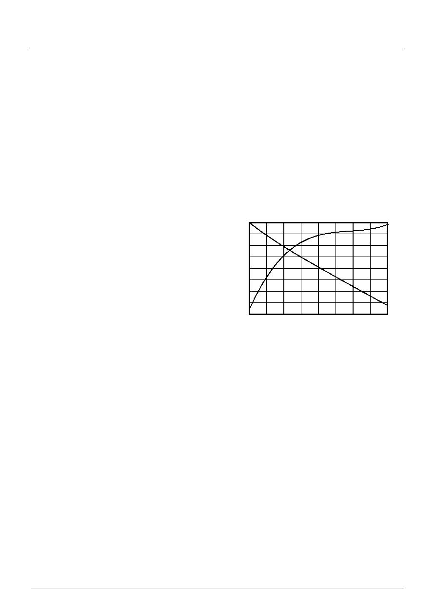
2.5. Temperature Sensor
Instead of the photodiode, a temperature dependent
resistor is used to generate the ADC input current.
Gain adjustment is not implemented in this cell. Tem-
perature data is accessed with the T_RD_FIRST com-
mand of the serial interface.
For accumulation time control, a separate counter is
necessary to achieve independence of the ACCUCTR
value. The divider value for this counter is fixed.
Temperature characteristic of the temperature sensor
can be seen in (see Fig. 2≠4 on page 9).
The temperature sensor is intended for relative tem-
perature measurements.
Fig. 2≠4: Temperature characteristic of temperature
sensor
2.6. Biasing and Reference Circuit
This circuit provides the reference voltage for the
ADCs and other internally needed bias voltages.
A "double bandgap" circuit provides a temperature-
compensated reference voltage of 2.5V and some ref-
erence currents. The reference voltage is used as
ADC reference. It is connected to the output pin
AGNDC. Reference currents are used to bias the
whole analog circuitry.
2.7. Voltage Regulator for Counter/Shifter Cells
To minimize interference from the ADC digital part and
the readout data shift registers to the ADC analog
parts, these digital blocks are supplied by a lower volt-
age than the other digital parts. The voltage regulator
provides this lower voltage. It has a value of 1.6V and
is supplied by the digital supply V
SUPD
.
0
20
40
60
Temp. [∞C]
30000
34000
38000
42000
n [coun
ts]
-
240
-
220
-
200
-
180
-1
60
dn/d
T
[co
unts/K
]

OPT
0
2
56C
A
D
V
A
NCE
INFORM
A
T
ION
10
May
15,
2002;
6251-581-1A
I
M
i
c
r
o
nas
Fig. 2≠5: Signals in different modes
MODE EXT_START
MOSI
START
HiZ
DATA
DATA
DATA
DATA
DATA
DATA
HiZ
DATA
DATA
HiZ
0
1
1
0
255
254
1
0
MODE
EXT_START
START
HiZ
DATA
DATA
DATA
DATA
DATA
HiZ
DATA
DATA
HiZ
0
1
1
0
255
254
0
ACCUCOUNTER=0
DAVQ
MISO
START_ACQ
MODE CONT
MOSI
ACCUCOUNTER=0
DAVQ
MISO
START_ACQ
START
MODE
EXT_START_
START
READ
READ
READ
HiZ
DATA
DATA
DATA
D_RD_FIRST
D_RD_NEXT
D_RD_TERM
255
254
0
MODE EXT_START_STOP
MOSI
ACCUCOUNTER=0
DAVQ
MISO
START_ACQ
STOP
STOP
HiZ
DATA
DATA
DATA
HiZ
255
254
0
READ
D_RD_NEXT
READ
D_RD_FIRST
READ
D_RD_NEXT
READ
D_RD_NEXT
READ
D_RD_TERM
READ
READ
D_RD_FIRST
D_RD_NEXT
READ
D_RD_TERM
READ
D_RD_NEXT
READ
D_RD_FIRST
READ
D_RD_NEXT
READ
D_RD_NEXT
READ
D_RD_FIRST
READ
D_RD_NEXT
READ
D_RD_NEXT
READ
D_RD_FIRST
READ
D_RD_NEXT
READ
D_RD_NEXT
READ
D_RD_TERM
READ
D_RD_NEXT
READ
D_RD_FIRST
READ
D_RD_NEXT
READ
D_RD_NEXT
READ
D_RD_FIRST
READ
D_RD_NEXT
READ
D_RD_NEXT
MODE
CONT
MODE
CONT
ADVANCE INFORMATION
OPT 0256C
Micronas
May 15, 2002; 6251-581-1AI
11
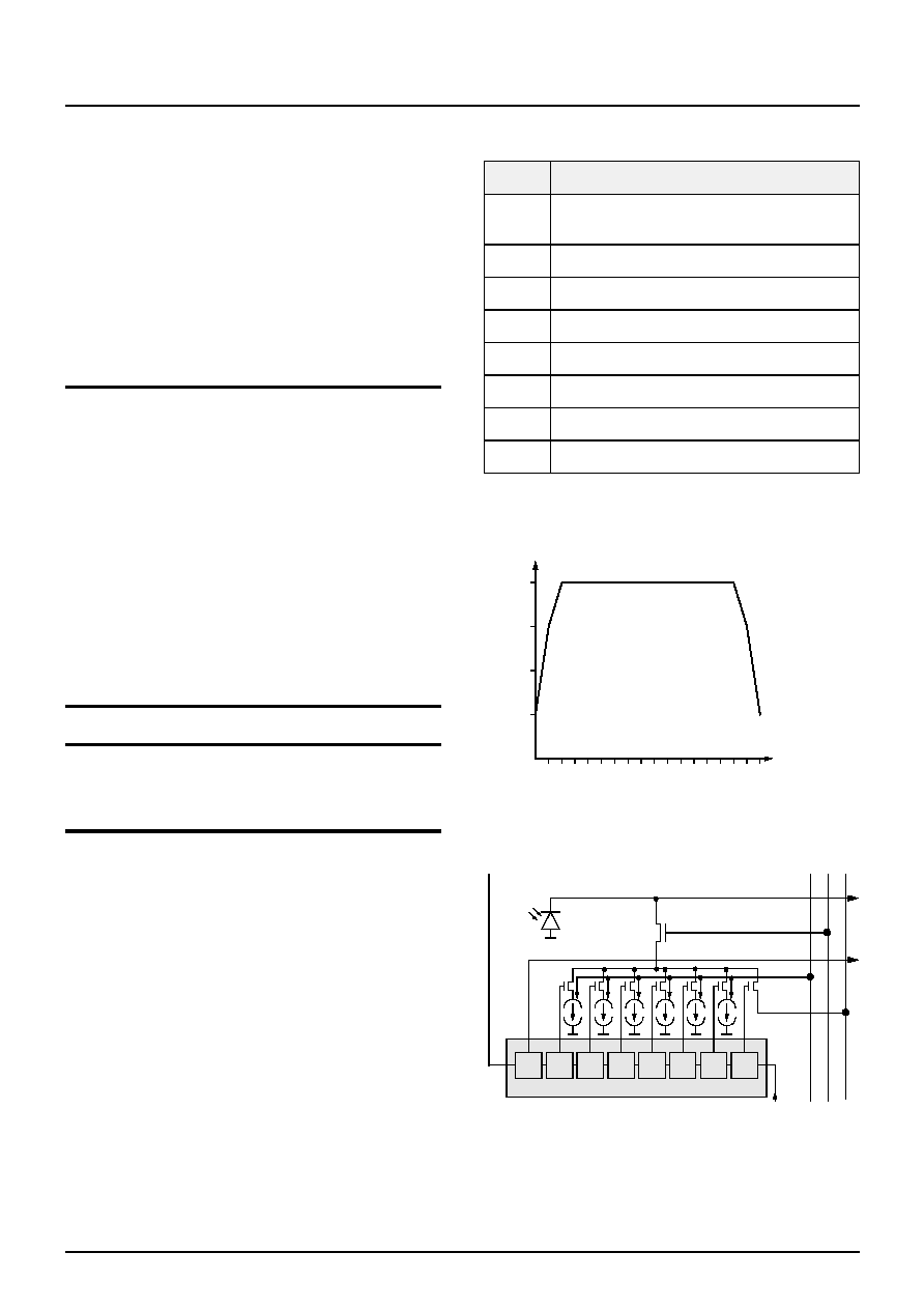
2.8. Current Adder
To provide the possibility of testing most parts of the
chip without optical stimulation, a current adder is inte-
grated for each channel. It consists of six weighted
current sources, see (see Fig. 2≠1 on page 4). To flat-
ten the ADC response with flat response disabled, a
global current source is selectable for a single channel
at the same time. Additionally, the respective ADC can
be completely deactivated. This can be used for char-
acterization but also in normal operation to reduce
measurement interference (i.e. to measure small parts
of the spectrum).
Note: The current value for each channel is selected
with the serial interface command ADCUR_WR.
This command is similar to the configuration
command GAIN_WR. Beginning with data for
channel 0 after reset, each data bit of
ADCUR_WR commands is shifted in the current
adder shift register.
The first part of the current adder shift register
belongs to the temperature sensor. Therefore,
this shift register has 257
◊
8 bits. To fill up this
shift register i.e. 172 ADCUR_WR 16-bit com-
mands are necessary. The first 8 bits of the first
ADCUR_WR command are dummies in this
case and will be shifted out at the end of the
172
th
ADCUR_WR command; the last 8 bits
determine the current adder value of the tem-
perature sensor.
Note: The first data bit of the command CURADD
determines whether the respective ADC is
enabled or not (1=disabled, 0=enabled). The
reset value is 0=enabled.
The current sources are weighted, see Table 2≠2. Due
to current source mismatch, the weighting factors are
approximations, only. The achieved measure point
density is not constant over the whole ADC range.
There are less measurement points in the upper and
lower region (see Fig. 2≠6). The Input ADCURIN
serves as current reference input. Thus it is possible to
adjust the current sources to the ADC's full-scale. A
small reference current I
REFINT
(approx. 10
µ
A) for the
current adder is generated internally. This offers the
possibility to use the current adder function to deter-
mine the relative ADC gain values for different gain
selections in standard application environment. The
pin ADCURIN has to be connected to ground in this
case.
Fig. 2≠6: Measure point density over ADC range
Fig. 2≠7: Current adder
Table 2≠2: Current source weighting
Bit
Weighting of Current Source
0
Global Current Source
6
◊
(I
ADCURIN
+I
REFINT
)
◊
27.78
◊
10
-
6
1
1
◊
(I
ADCURIN
+I
REFINT
)
◊
27.78
◊
10
-
6
2
1
◊
(I
ADCURIN
+I
REFINT
)
◊
27.78
◊
10
-
6
3
1
◊
(I
ADCURIN
+I
REFINT
)
◊
27.78
◊
10
-
6
4
2
◊
(I
ADCURIN
+I
REFINT
)
◊
27.78
◊
10
-
6
5
4
◊
(I
ADCURIN
+I
REFINT
)
◊
27.78
◊
10
-
6
6
8
◊
(I
ADCURIN
+I
REFINT
)
◊
27.78
◊
10
-
6
7
Enable (0) / Disable (1) respective ADC
0
Density
FS
ADC
Range
Current Adder Shift Register
MSB
LSB
Photodiode
to ADC
ADCURIN
1
1
1
2
4
8
CURADD
disable ADC
Igl
o
b
a
l
OPT 0256C
ADVANCE INFORMATION
12
May 15, 2002; 6251-581-1AI
Micronas
3. Specifications
3.1. Package for Evaluation Purposes
The specified package is intended for evaluation pur-
poses only.
Packaging depends strongly on the application. Con-
tact Micronas for appropriate packaging.
3.2. Outline Dimensions (Preliminary)
Fig. 3≠1: 48-Pin Ceramic Dual In-Line Package with 0.05" pitch
SENSOR AREA
1.6
4.
1
14.59
15.5
30.5
25
24
1
48

ADVANCE INFORMATION
OPT 0256C
Micronas
May 15, 2002; 6251-581-1AI
13
3.3. Pin Connections and Short Descriptions
NC = not connected, leave vacant
LV = if not used, leave vacant
V
SUPD
= if not used, connect to V
SUPD
X = obligatory; connect as described in circuit diagram
Pin No.
Pin Name
Type
Connection
Short Description
1
COUNTIN_1/2
IN
GND
D
test input
1)
2
PCSENQ_1/2
IN
X
peripheral chip select
3
MCLK_1/2
IN
X
main clock input
4
SCLK_1/2
IN
X
gated serial clock
5
MOSI_1/2
IN
X
serial data input
6
PFMOUT_1/2
OUT
LV
test output
1)
7
DAVQ_1/2
OUT
LV
data available (low active)
8
V
SUPS
_1/2
SUPPLY
X
internal gen. counter/shifter supply
9
GND
S
_1/2
SUPPLY
X
counter/shifter ground
10
GND
D
_1/2
SUPPLY
X
digital ground
11
V
SUPD
_1/2
SUPPLY
X
digital supply
12
MISO_1/2
OUT
X
serial data output
13
GND
BP
_1/2
SUPPLY
GND
A
back plate ground
14
START_ACQ_1/2
IN
V
SUPD
start accumulation (low active)
15
TESTCLK_1/2
IN
GND
D
test input
1)
16
RESETQ_1/2
IN
X
reset signal (low active)
17
V
SUPB
_1/2
SUPPLY
X
ADC clock buffer supply
18
GND
B
_1/2
SUPPLY
X
ADC clock buffer ground
19
GND
A
_1/2
SUPPLY
X
analog ground
20
V
SUPA
_1/2
SUPPLY
X
analog supply
21
AGNDC_1/2
OUT(IN)
X
ADC reference voltage
22
BUFREF_1/2
SUPPLY
X
buffered reference voltage
23
ADCURIN_1/2
IN
GND
A
additional current adder input
1)
24
V
SUPA
_1/2
SUPPLY
LV
2
nd
connection to analog supply
1)
for test purposes, only

OPT 0256C
ADVANCE INFORMATION
14
May 15, 2002; 6251-581-1AI
Micronas
3.4. Pin Descriptions
Pin 1, COUNTIN
test input.
Pin 2, PCSENQ
peripheral chip select (low-active). This signal
switches the MISO pin to high-impedance state and
determines the length of input data frames.
Pin 3, MCLK
main clock input
Pin 4, SCLK
gated serial clock from master SPI interface. This
clock signal should be derived from the main clock
MCLK with an integer division factor.
Pin 5, MOSI (Master Out Slave In)
serial data input from master SPI interface.
Pin 6, PFMOUT
test output
Pin 7, DAVQ
data available (low active). This pin serves as an inter-
rupt signal. It is set to low at the and of each accumula-
tion cycle and is set to high by the serial interface com-
mands IRQ_ACKN and D_RD_FIRST.
Pin 8, V
SUPS
internally generated counter/shifter supply. This pin
intended to be connected to a blocking capacitance,
only. Use a capacitor with low ESR. Do not connect
this pin with an external supply.
Pin 9, GND
S
ground of internally generated counter/shifter supply.
This pin should be connected low-resistive and low-
inductive with the common board ground like any other
ground pin.
Pin 10, GND
D
digital ground
Pin 11, V
SUPD
digital supply
Pin 12, MISO (Master In Slave Out)
serial data output to master SPI interface.
Pin 13, GND
BP
back plate ground
Pin 14, START_ACQ
low active start/stop signal. In MODE CONT, a falling
edge on this pin starts the first accumulation cycle. In
MODE EXT_START, a falling edge starts a new accu-
mulation cycle. In MODE EXT_START_S, a falling
edge starts a new accumulation cycle, a rising edge
stops the current accumulation cycle.
Pin 15, TESTCLK test input
Pin 16, RESETQ
hardware reset (low active)
Pin 17, V
SUPB
supply for ADC clock buffer
Pin 18, GND
B
ground for ADC clock buffer
Pin 19, GND
A
analog ground
Pin 20, V
SUPA
analog supply
Pin 21, AGNDC
internally generated reference voltage input and out-
put. By connecting a capacitor, a low pass filter is
achieved with the internal 120k resistor connected in
series to the reference voltage source.
Pin 22, BUFREF
buffered reference. This pin intended to be connected
to a blocking capacitance, only. Use a capacitor with
low ESR.
Pin 23, ADCURIN
current input for current adder. A positive input current
can additionally be applied for test purposes.
Pin 24, V
SUPA
analog supply (2
nd
connection)
ADVANCE INFORMATION
OPT 0256C
Micronas
May 15, 2002; 6251-581-1AI
15
3.5. Pin Configuration
Fig. 3≠2: 48-Pin Ceramic Dual In-Line Package with 0.052" pitch
COUNTIN
PCSENQ
MCLK
SCLK
MOSI
PFMOUT
DAVQ
V
SUPS
GND
S
GND
D
V
SUPD
MISO
GND
BP
START_ACQ
TESTCLK
RESETQ
V
SUPB
GND
B
GND
A
V
SUPA
AGNDC
BUFREF
ADCURIN
V
SUPA
35
30
25
20
15
24
15
10
40
4
5
48
S
E
NSOR AREA
S
E
NSOR AREA
S
E
NSOR AREA
OPT 0256C
ADVANCE INFORMATION
16
May 15, 2002; 6251-581-1AI
Micronas
3.6. Pin Circuits
Fig. 3≠3: Input pins RESETQ, SCLK, MOSI,
PCSENQ, MCLK, ENADCUR, SELPFMLA,
SELPFMCK
Fig. 3≠4: Output pins DAVQ, PFMOUT
Fig. 3≠5: Output pin MISO
Fig. 3≠6: Input pin ADCURIN
Fig. 3≠7: Output (Input) pins BUFREF, VSUPS
Fig. 3≠8: Output (Input) pin AGNDC7
V
SUPD
GND
D
GND
D
P
N
V
SUPD
GND
D
P
N
V
SUPD
High_Z
MISO
driver
P
V
SUPA
N
ADCURIN
GND
A
P
P
P
V
SUP
pin
AGNDC
GND
A
Bandgap
Voltage
Reference
120 k
to ADCs

ADVANCE INFORMATION
OPT 0256C
Micronas
May 15, 2002; 6251-581-1AI
17
3.7. Characteristics
3.7.1. Absolute Maximum Ratings
Stresses beyond those listed in the "Absolute Maximum Ratings" may cause permanent damage to the device. This
is a stress rating only. Functional operation of the device at these or any other conditions beyond those indicated in
the "Recommended Operating Conditions/Characteristics" of this specification is not implied. Exposure to absolute
maximum ratings conditions for extended periods may affect device reliability.
3.7.2. Recommended Operating Conditions
Symbol
Parameter
Pin Name
Min.
Max.
Unit
T
A
Ambient Operating Temperature
-
-
40
125
o
C
T
S
Storage Temperature
-
-
40
125
o
C
V
SUP
Supply Voltage, all Supply Inputs
V
SUPx
-
0.3
6
V
V
I
Input Voltage
All Inputs
-
0.3
V
SUP
+0.3
V
V
O
Output Voltage
All Outputs
-
0.3
V
SUP
+0.3
V
H
A
Humidity, non condensing
-
0
95
%
Symbol
Parameter
Pin Name
Min.
Typ.
Max.
Unit
T
A
Ambient Operating Temperature
-
0
-
60
o
C
V
SUPD/SUPP
Supply Voltage for Digital Blocks
V
SUPD/SUPP
3.15
3.30
3.45
V
V
SUPA
Supply Voltage for Analog Blocks
V
SUPA
4.75
1)
5.0
1)
5.25
1)
V
f
MCLK
Master Clock Frequency
2)
MCLK
-
5.24288
5.5
MHz
f
SCLK
Serial Clock Frequency
3)
SCLK
-
f
MCLK
t
CLK_h
/t
CLK_l
SCLK/MCLK High to Low Ratio
SCLK, MCLK
45
50
55
%
ACCUCTR
Accumulation Counter Value
-
128
2
16
-
2
2
26
-
1
counts
n
clk_acc_rstrt
Clock Cycles between Restart of
Accumulation Counter
4)
START_ACQ
2
1) Keep analog supply voltage ripple as low as possible
2) Frequency changes during operation are not allowed
3) A small area of phase relations will cause non recoverable data readout problems. This area is very small (<1ns)
and varies with temperature and supply voltage. To avoid corrupted output data make sure that the phase condition
in above figure is never true.
4) For external start and external start/stop mode only
MCLK
SCLK
1ns
3ns
avoid negative SCLK edges in this area
(3 ns to 1 ns before negative MCLK edge)

OPT 0256C
ADVANCE INFORMATION
18
May 15, 2002; 6251-581-1AI
Micronas
3.7.3. Electrical Characteristics
At V
SUPA/B
= 5 V, V
SUPD
= 3.3 V, T = 27
o
C, gain = 1
Symbol
Parameter
Pin Name
Min.
Typ./
Max.
Unit
Test Conditions
P
TOT
Total Power Dissipation
-
130
200
mW
ADC full scale
I
VSUPD
Current Consumption
V
SUPD
-
2.6
12
mA
ADC full scale
I
VSUPB
Current Consumption
V
SUPB
-
1.2
2
mA
I
VSUPA
Current Consumption
V
SUPA
-
25
70
mA
ADC full scale
I
L_I/O
I/O Leakage Current
All I/O Pins
-
1
1
µ
A
V
OL
Output Low Voltage
DAVQ,
0.4
V
I
OL
= 1.5 mA
V
OH
Output High Voltage
PFMOUT
2.4
V
I
OL
=
-
1.5 mA
t
OT
Output Transition Time
8
ns
C
LOAD
= 30 pF
V
OL,MISO
Output Low Voltage
MISO
0.4
V
I
OL
= 2 mA
max. driver ($0F)
V
OH,MISO
Output High Voltage
2.4
V
I
OL
=
-
2 mA
max. driver ($0F)
t
OT,MISO
Output Transition Time
5
ns
C
LOAD
= 30 pF
max. driver ($0F)
V
IL
Input Low Voltage
All I Pins
0.8
V
V
IH
Input High Voltage
All I Pins
2.0
V
I
PH
Photo Current Range
-
0
25
nA
I
FS
Full Scale Photo Current
-
20.4
9.14
4.30
1.98
23.3
= 3.7%
10.7
= 4.0%
5.27
= 4.6%
2.63
= 5.6%
26.2
12.26
6.24
3.28
nA
gain = 0
gain = 1
gain = 2
gain = 3
V
AGNDC
Reference Voltage
AGNDC
2.4
2.5
2.6
V
Load Impedance
> 10 M
e
STAB
Stability Error
1)
-
-
4
4
10
-
5
1% / 99% Quantiles
of I
FS
relative to its
mean value I
FS
within 1 h
measurement
duration at constant
temperature
m
neighbour
Gain Matching Between
Neighboring Cells
2)
-
0.85
0.9
0.93
0.95
= 3.0%
s = 2.0%
s = 1.4%
= 1.0%
1.15
1.1
1.07
1.05
gain = 0
gain = 1
gain = 2
gain = 3
m
random
Gain Matching Between
Random Cells
3)
-
0.775
0.845
0.895
0.925
= 4.5%
s = 3.1%
s = 2.1%
= 1.5%
1.225
1.155
1.105
1.075
gain = 0
gain = 1
gain = 2
gain = 3
n
DIG
I
PH
------------
f
MCLK
t
ACC
I
F S
-------------------------------
=

ADVANCE INFORMATION
OPT 0256C
Micronas
May 15, 2002; 6251-581-1AI
19
3.7.4. Geometrical Characteristics
INL
Integral Nonlinearity Error
-
-
-
1
%FS
flat response = off
4)
DNL
Differential Nonlinearity
1)
-
-
-
2
LSB
TK
I
FS
Temperature Coefficient
1)
-
-
-
0.05
%/K
flat response = on
-
-
0.15
0
0.15
flat response = off
N
RMS
RMS Noise of n
DIG
-
4
6
9
15
LSB
gain = 0, 75% of FS
gain = 1, 75% of FS
gain = 2, 75% of FS
gain = 3, 75% of FS
c
TempSensor
Temperature Sensor
Coefficient
1)
-
-
-
0.577
%/K
@27
o
C
n
TempSensor
Temperature Sensor Value
-
24300
30000
35700
counts
@27
o
C
1) Measuring these values is not part of the production test
2) With m
neighbour
= I
FSn
/[(I
FSn
+I
FSn+1
)/2]
3) With m
random
= I
FSn
/I
FS
4) With flat response = on the specified value is only valid to 70% ADC FS.
Symbol
Parameter
Pin Name
Min.
Typ./
Max.
Unit
Test Conditions
Symbol
Parameter
Min.
Typ.
Max.
Unit
N
C
Number of Channels
-
256
-
d
H
Pixel Height of Photodiode
-
1600
-
µ
m
d
P
Channel Pitch
-
50
-
µ
m
d
G
Gap Between Photodiodes
5
µ
m
l
die
Chip length
14.6
mm
h
die
Chip height
4.1
mm
d
W
Wafer Thickness
375
390
405
d
OX
Thermal Oxide Thickness over Photodiodes
385
430
475
nm

OPT 0256C
ADVANCE INFORMATION
20
May 15, 2002; 6251-581-1AI
Micronas
3.7.5. Optical and Electro-optical Characteristics
Symbol
Parameter
Min.
Typ.
Max.
Unit
Test Conditions
l
Wavelength Range
1)
190
-
1100
nm
PD
Quantum Efficiency of Photodiode
1)
20
40
60
40
20
%
= 200 nm
= 350 nm
= 650 nm
= 800 nm
= 900nm
|
Iph
|
Temperature Coefficient of Photo
Current
1)
0.2
0.1
0.5
%/K
= 200 nm
= 500 nm
= 900 nm
I
L_PD
Photodiode Leakage Current
0.2
1
pA
T
junction
= 27
o
C
L_PD
Temperature Exponent Of I
L_PD
2)
22.2
XTALK
Channel to Channel Crosstalk
1)
0.4
2
%FS
t
dark, 10 pA
Input Step Response Time from Dark
to I
ph
= 10 pA
1)
10
20
ms
settling within
±
10% of final
value
t
bright, 10 pA
Input Step Response Time from Bright
to I
ph
= 10 pA
1)
3
8
ms
settling within
±
10% of final
value
t
settling
Settling Time
1)3)
100
ms
within 0.01%
of final value
@t
dark
> 10 min
1) Measuring these values is not part of the production test
2)
With I
L_PD
(T) = I
L_PD
(T
0
)*(T/T
0
)
L_PD
3) Transient behavior and settling time may depend on length of dark phase before dark/light transition.

ADVANCE INFORMATION
OPT 0256C
Micronas
May 15, 2002; 6251-581-1AI
21
3.7.6. UV Degradation
Symbol
Parameter
Min.
Typ.
Max.
Unit
Test Conditions
Ph
Photo Degradation
15*
10
-
9
m
2
/Ws
= 200 nm
1)
1) Photo Degradation may occur under strong UV irradiation. Photo Degradation is defined by the loss of sensitivity
cause by an exposure dose on the pixel area at a specific irradiation wavelength.
Assumptions for typical operating conditions at
= 200 nm:
Requirements: less than 30% loss of sensitivity @
= 200 nm after 3 years of typical operation (3000h/a)
The effect of photo degradation is proportional to exposure density and has a logarithmic dependency on exposure
wavelength. The photo degradation rate rises approximately by one order of magnitude every 25 nm towards lower
wavelengths.
*)
:Mean exposed area
Ph
loss of sensitivity
exposure dose density
-----------------------------------------------------
sensitivity
sensitivity
------------------------
expose
t
exp
A
exp
------------------------------
------------------------------
0,3
25nW 3,2 10
7
s
4 10
8
≠
m
2
------------------------------------------
------------------------------------------
15 10
9
≠
m
2
Ws
--------
=
=
=
=
I
PH
2,5nA; sensitivity
0,1
A
W
----- A
exp
;
50
µ
m 800
*)
µ
m
4 10
8
≠
m
2
=
=
=
=
expose
I
PH
sensitivity
---------------------------
2,5nA
0,1
A
W
-----
---------------
25nW
=
=
=
sensitivity
sensitivity
------------------------
0,3 t
exp
;
3,2 10
7
s
=
=

OPT 0256C
ADVANCE INFORMATION
22
May 15, 2002; 6251-581-1AI
Micronas
4. Application Notes
4.1. Data Read Out
Reading out data from the respective shift registers
can lead to interference of the ADCs. To minimize the
interference, a minimal SCLK frequency should be
used.
The minimum possible serial clock frequency can be
achieved by selecting
The minimum SCLK frequency is therefore
In the continuous mode MODE CONT, a command
sequence of 1
◊
D_RD_FIRST and 255
◊
D_RD_NEXT
can then be used to get the data of all channels. The
signal DAVQ can be ignored.
4.2. Blocking Capacitors
To avoid loss of performance due to supply voltage rip-
ple, all supply pins have to be connected with blocking
capacitors.
A combination of lower capacitances in the range of
10 nF...100 nF for higher frequency interference and
higher capacitances in the range of 1
µ
F...100
µ
F for
lower frequency interference is recommended. The
wires which connect the 10 nF...100 nF capacitors to
the IC should be of minimum length.
4.3. Cascading
More than one OPT 0256C IC can be connected in
parallel to one master SPI-compatible interface. The
wires SCLK, MISO, and MOSI can be connected
together. For PCSENQ and DAVQ, separate outputs/
inputs of the master have to be used.
Note: Higher SCLK frequencies due to cascading of
OPT 0256C ICs may cause a loss of perfor-
mance, see section (see Section 4.1. on
page 22).
Fig. 4≠1:
Application circuit example with both PDAs of an OPT 0256C IC connected to one SPI master
ACCUCTR
n
256 16
(
)
∑
2
≠
=
f
SCLK
f
MCLK
256
16
2
+
(
)
ACCUCTR
1
+
-----------------------------------------------------
=
Master
SCLK
MOSI
MISO
Master Clock
PCSENQ
CLOCK
Start Acquisition
DAVQ
Reset
Analog Supply 5V
Board Ground
Digital Supply 3.3V
COUNTIN
PCSENQ
MCLK
SCLK
MOSI
PFMOUT
DAVQ
V
SUPS
GND
S
GND
D
VSUP
D
MISO
GND
BP
START_ACQ
TESTCLK
RESETQ
V
SUPB
GND
B
GND
A
V
SUPA
AGNDC
DUMPDRAIN
ADCURIN
V
SUPA
4.7nF
10
µ
F
10
µ
F
4.7nF
4.7nF
10
µ
F
4.7nF
10
µ
F
10
µ
F
4.7nF
4.7nF
10
µ
F

ADVANCE INFORMATION
OPT 0256C
Micronas
May 15, 2002; 6251-581-1AI
23

All information and data contained in this data sheet are without any
commitment, are not to be considered as an offer for conclusion of a
contract, nor shall they be construed as to create any liability. Any new
issue of this data sheet invalidates previous issues. Product availability
and delivery are exclusively subject to our respective order confirmation
form; the same applies to orders based on development samples deliv-
ered. By this publication, Micronas GmbH does not assume responsibil-
ity for patent infringements or other rights of third parties which may
result from its use.
Further, Micronas GmbH reserves the right to revise this publication
and to make changes to its content, at any time, without obligation to
notify any person or entity of such revisions or changes.
No part of this publication may be reproduced, photocopied, stored on a
retrieval system, or transmitted without the express written consent of
Micronas GmbH.
OPT 0256C
ADVANCE INFORMATION
24
May 15, 2002; 6251-581-1AI
Micronas
Micronas GmbH
Hans-Bunte-Strasse 19
D-79108 Freiburg (Germany)
P.O. Box 840
D-79008 Freiburg (Germany)
Tel. +49-761-517-0
Fax +49-761-517-2174
E-mail: docservice@micronas.com
Internet: www.micronas.com
Printed in Germany
Order No. 6251-581-1AI
5. Data Sheet History
1. Advance Information: "OPT 0256C Photo Detector
Array IC", May 15, 2002, 6251-581-1AI. First
release of the advance information.