PUC 303xA
PRELIMINARY DATA SHEET
2
April 2, 2002; 6251-565-1PD
Micronas
Contents
Page
Section
Title
5
1.
Introduction
5
1.1.
Features
5
1.2.
Application Overview
6
2.
Functional Description
6
2.1.
Device Overview
6
2.1.1.
64-MHz ARM7TDMI
6
2.1.2.
48 + 8 kByte SRAM
6
2.1.3.
256 kByte Embedded Flash
6
2.1.4.
Memory Protection Unit
6
2.1.5.
Power Management Unit
6
2.1.6.
12-Mbit/s USB 1.1 Function Core
6
2.1.7.
66 General-Purpose I/Os
6
2.1.8.
5 x Synchronous Serial Port
6
2.1.9.
2 x UARTs / IrDA
6
2.1.10.
3 x Timer / Counters
6
2.1.11.
Watchdog
6
2.1.12.
Interrupt Controller
6
2.1.13.
Real Time Clock
7
2.2.
ARM7TDMI Processor and AHB/APB Buses
7
2.2.1.
Memory Map
8
2.3.
Clock Generation
11
2.3.1.
Clock Utilization Summary
12
2.3.2.
Phase-Locked Loop Device
13
2.4.
Power-on and Resets
15
2.5.
AHB Peripherals
15
2.5.1.
Flash Memory
15
2.5.1.1.
Flash Memory Map
16
2.5.1.2.
Flash Configuration Registers
19
2.5.1.3.
Flash Features
19
2.5.1.4.
Programmable Wait States
19
2.5.1.5.
Flash Programming and Erasing
20
2.5.2.
Security of Application Code
20
2.5.3.
SRAM
20
2.5.3.1.
Features
20
2.5.3.2.
General Overview
21
2.5.4.
Memory Protection Unit
21
2.5.4.1.
SRAM Remapping
21
2.5.4.2.
MPU Address Space
24
2.5.5.
USB Interface
26
2.6.
APB Peripherals
26
2.6.1.
Power Management Unit
26
2.6.1.1.
Power States
27
2.6.1.2.
Power Management Register Descriptions

Contents, continued
Page
Section
Title
PRELIMINARY DATA SHEET
PUC 303xA
Micronas
April 2, 2002; 6251-565-1PD
3
37
2.6.2.
Interrupt Controller
37
2.6.2.1.
Features
37
2.6.2.2.
Interrupt List
38
2.6.2.3.
General Overview
38
2.6.2.4.
Programming Guide
40
2.6.2.5.
Interrupt Controller Register Definitions
48
2.6.3.
UARTs
48
2.6.3.1.
Features
48
2.6.3.2.
UART Functions
50
2.6.3.3.
UART Register Map
65
2.6.4.
Synchronous Serial Ports
65
2.6.4.1.
SSP Peripheral Operation
66
2.6.4.2.
SSP Modes
66
2.6.4.3.
SSP Primary Modes
67
2.6.4.4.
SSP Secondary Modes
68
2.6.4.5.
Example SSP Communication Waveforms
70
2.6.4.6.
SSP Register Descriptions
79
2.6.4.7.
SSP Interrupt Logic
80
2.6.5.
Timers
80
2.6.5.1.
Features
80
2.6.5.2.
Description
81
2.6.5.3.
Initialization
81
2.6.5.4.
Modes of Operation
82
2.6.5.5.
Generation of Waveforms
83
2.6.5.6.
TTC Register Descriptions
89
2.6.6.
Real Time Clock
89
2.6.6.1.
Features
89
2.6.6.2.
Description
89
2.6.6.3.
Standby Mode
89
2.6.6.4.
Register Map and Formats
98
2.6.6.5.
Programming Instructions
101
2.6.7.
Watchdog Timer
101
2.6.7.1.
Features
101
2.6.7.2.
Description
102
2.6.7.3.
Watchdog Register Descriptions
102
2.6.7.4.
Watchdog Timer Reset
102
2.6.7.5.
Watchdog Timer Enable Sequence
106
2.6.8.
General Purpose I/O Module
106
2.6.8.1.
Features
106
2.6.8.2.
Description
106
2.6.8.3.
Bypass Mode
106
2.6.8.4.
Interrupts
107
2.6.8.5.
Signal Interface
107
2.6.8.6.
Initialization
107
2.6.8.7.
GPIO Address Map
107
2.6.8.8.
Programming Interface

PUC 303xA
PRELIMINARY DATA SHEET
4
April 2, 2002; 6251-565-1PD
Micronas
Contents, continued
Page
Section
Title
109
3.
Specifications
109
3.1.
Outline Dimensions
110
3.2.
Pin Connections and Short Descriptions
114
3.3.
Pin Descriptions
114
3.3.1.
Special Function Pins
115
3.3.2.
Shared GPIO / Special Function Pins
115
3.3.3.
General Purpose I/O Pins Without Special Function
118
3.4.
Pin Circuits
119
3.5.
Electrical Characteristics
119
3.5.1.
Absolute Maximum Ratings
120
3.5.2.
Recommended Operating Conditions
121
3.5.3.
Power Consumption
123
3.5.4.
DC Characteristics
123
3.5.4.1.
Digital Outputs
123
3.5.4.2.
Hysteresis of Schmitt Trigger Inputs
123
3.5.4.3.
Internal Pull-up / Pull-down Resistor Values
124
3.5.5.
AC Characteristics
124
3.5.5.1.
SSP Slave (SCLKx and SFRMx are Inputs)
124
3.5.5.2.
SSP Master (SCLKx and SFRMx are Outputs)
125
3.5.5.3.
Timing Diagrams
126
3.5.5.4.
AC Characteristics for CLKOUT Pin
126
3.5.5.5.
Timing Requirement for WAKE_UP Pin
126
3.5.5.6.
Timing Requirement for TIMER_x Inputs
126
3.5.5.7.
Timing Requirement for GPIO Inputs
126
3.5.5.8.
Rise/Fall Times of 4-mA and 12-mA Outputs
127
3.5.6.
Flash Programming Characteristics
129
4.
List of Abbreviations
130
5.
Data Sheet History
PRELIMINARY DATA SHEET
PUC 303xA
Micronas
April 2, 2002; 6251-565-1PD
5
Programmable Universal Controller
1. Introduction
The Programmable Universal Controller PUC 303xA is
ideally suited for use in portable consumer devices. It
is equipped with an embedded ARM7TDMI processor,
a highly flexible power management scheme, and
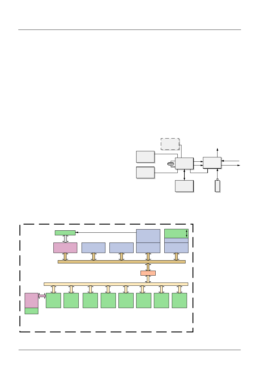
embedded Flash. Fig. 1≠2 shows a simplified func-
tional block diagram of the PUC 303xA.
1.1. Features
≠ 64-MHz ARM7TDMI
≠ 48 kByte embedded SRAM
≠ 256 kByte embedded Flash
≠ Memory Protection Unit
≠ Secure Mode Controller
≠ Power Management Unit with integrated PLL
≠ 12 Mbit/s USB 1.1 function core with integrated
transceiver (PUC 3030A only) and dedicated
8 kByte SRAM
≠ I
2
C Master/Slave interface
≠ 66 General-purpose I/Os
≠ 5
◊
Synchronous Serial Port (including I
2
S master),
24 Mbit/s max. speed as master, 16 Mbit/s max.
speed as slave.
≠ 2
◊
UARTs / IrDA
≠ 3
◊
timer / counter
≠ Watchdog
≠ Interrupt Controller with hardware prioritization
≠ Real Time Clock (not available for all packages)
≠ Especially suited to interface with Micronas'
MAS 35x9F / MAS 3587F / SAC 3590A devices
1.2. Application Overview
The PUC 303xA meets the requirements of digital
audio players, specific mobile network appliances, dig-
ital audio recorders (including water-marking and
DRM), and wireless applications such as BluetoothTM.
The PUC 303xA device offers appropriate security fea-
tures, embedded Flash, and a variety of communica-
tion interfaces, including USB connectivity.
Fig. 1≠1: Example application: multistandard secure
player /recorder
Fig. 1≠2: Simplified functional block diagram of the PUC 303xA (see also List of Abbreviations on page 129)
Memory Card
PUC 303xA
MAS 35x9F
MAS 3587F
LCD
Keyboard
I
2
C
I
2
S
Clock
Mic/Line-In
Headphone-Out
Supply-Out
PC
V_Bat-In
USB
SAC 3590A
e.g.
SC-Card
ARM7TDMI
MPU
SRAM
48 kByte
Prog. Flash
256 kByte
Security
Controller
USB
Transceiver
JTAG Port
USB I C
Function Core
8 kByte SRAM
2
Power
Manage-
ment Unit
2
◊
UARTs
with IrDA
Interrupt
Controller
5
◊
Sync
Serial
Ports
3
◊
Timer
Counters
66
◊
GPIO
Realtime
Clock
Watchdog
Clock
and
Reset
Control
PLL
Bridge
AHB
APB
AHB Advanced High-performance Bus
APB Advanced Peripheral Bus
ARM7TDMI ARM Processor Core
GPIO General Purpose Input/Output
MPU Memory Protection Unit
PLL Phase-Locked Loop
USB Universal Serial Bus