Micropac Industries cannot assume any responsibility for any circuits shown or represent that they are free from patent infringement.
Micropac reserves the right to make changes at any time in order to improve design and to supply the best product possible.
MICROPAC INDUSTRIES, INC. HYBRID MICROELECTRONICS PRODUCTS DIVISION
∑ 905 E. Walnut St., Garland, TX 75040 ∑ (972) 272-3571 ∑ Fax (972) 494-2281
www.micropac.com
E-MAIL:
hybridsales@micropac.com
05/16/01
42106
OPERATIONAL AMPLIFIER
DSCC DWG #5962-8762001
(Replacement for OP501, PA51)
Mii
HYBRID MICROELECTRONICS
PRODUCTS DIVISION
Features:
∑ Wide Supply Voltage Range (
±
10 to
±
40 Volts)
∑ High Output Current (10A Peak)
∑ Small Size (TO-3, 8 Pins)
∑ Low Cost
Applications:
∑ Valve and Actuator Control
∑ DC or AC Power Regulator
∑ Motor/Synchro Driver
∑ DC Servo Amplifier
DESCRIPTION
The 42106 is a high power, high voltage, high current, power operational amplifier and is a replacement for the PA51 &
OPA501. They are designed to drive capacitive, inductive and sensitive loads. The devices are complete with current
limiting using external resistors, and fabricated using hybrid techniques to maximize reliability, minimize size and give
top performance.
ABSOLUTE MAXIMUM RATINGS
Power Supply Voltage (V
CC
) .................................................................................................................................
±40VDC
Differential Input Voltage ......................................................................................................................................
±V
CC
-3V
Common Mode Input Voltage .....................................................................................................................................
±V
CC
Operating Temperature Range (case) .................................................................................................... -55∞C to +125∞C
Storage Temperature Range ................................................................................................................... -65∞C to +150∞C
Output Current .................................................................................................................................................... 10A Peak
Power Dissipation at T
C
= 25∞C ..................................................................................................................................97W
Lead Temperature (Soldering < 10 sec).................................................................................................................+300∞C

Micropac Industries cannot assume any responsibility for any circuits shown or represent that they are free from patent infringement.
Micropac reserves the right to make changes at any time in order to improve design and to supply the best product possible.
MICROPAC INDUSTRIES, INC. HYBRID MICROELECTRONICS PRODUCTS DIVISION
∑ 905 E. Walnut St., Garland, TX 75040 ∑ (972) 272-3571 ∑ Fax (972) 494-2281
www.micropac.com
E-MAIL:
hybridsales@micropac.com
05/16/01
42106
OPERATIONAL AMPLIFIER DESC DWG #5962-8762001
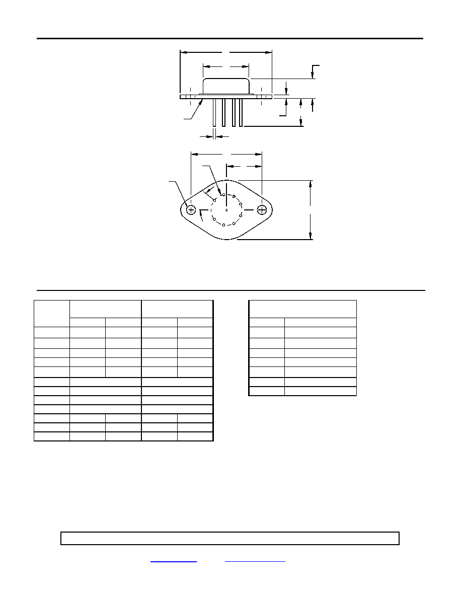
Mechanical Configuration
A
C
K
B
E
R
J
H
Q
G
D
SEATING PLANE
F
1
2 3
4
5
6
7
8
Note: Leads in true position with 0.010" (0.25mm) R at MMC at seating plane
Pin Numbers shown for reference only. Numbers may not be marked on package.
INCHES
MILLIMETERS
ELECTRICAL
CONNECTIONS
DIM
MIN
MAX
MIN
MAX
Pin 1
Output 1
A
1.510
1.550
38.35
39.37
Pin 2
CL
+
B
.745
.770
18.92
19.56
Pin 3
+V
C
C
.260
.300
6.60
7.62
Pin 4
+IN
D
.038
.042
0.97
1.07
Pin 5
-IN
E
.080
.105
2.03
2.67
Pin 6
-V
C
F
40∫ BASIC
40∫ BASIC
Pin 7
N.C.
G
.500 BASIC
12.7 BASIC
Pin 8
CL-
H
1.186 BASIC
30.12 BASIC
J
.583 BASIC
15.08 BASIC
K
.400
.500
10.16
12.70
Q
.151
.161
3.84
4.09
R
.980
1.020
24.89
25391

Micropac Industries cannot assume any responsibility for any circuits shown or represent that they are free from patent infringement.
Micropac reserves the right to make changes at any time in order to improve design and to supply the best product possible.
MICROPAC INDUSTRIES, INC. HYBRID MICROELECTRONICS PRODUCTS DIVISION
∑ 905 E. Walnut St., Garland, TX 75040 ∑ (972) 272-3571 ∑ Fax (972) 494-2281
www.micropac.com
E-MAIL:
hybridsales@micropac.com
05/16/01
42106
OPERATIONAL AMPLIFIER DESC DWG #5962-8762001
ELECTRICAL CHARACTERISTICS
T
C
= 25∞ C, V
CC
=
±
36 VDC
unless otherwise specified
PARAMETER
SYMBOL
TEST CONDITIONS
MIN
TYP
MAX
UNIT
Input Offset Voltage
V
IO
T
C
= 25∞C
T
C
= -55∞C to +125∞C
±5
±40
mV
uV/∫C
Input Offset Voltage vs
Supply
V
IO
(V
CC
)
±35
µV/V
Input Offset Voltage vs
Power
V
IO
(P)
±20
µV/W
Input Bias Current
I
B+
, I
B-
T
C
= 25∞C
T
C
= -55∞C to +125∞C
.05
20
nA
nA/∞C
Input Bias Current vs
Supply
I
B
(V
CC
)
.02
nA/V
Input Offset Current
I
I0
T
C
= 25∞C
T
C
= -55∞C to +125∞C
.01
3
nA
nA/∞C
Input Impendance
R
IN
250
M
Gain Bandwidth Product
@ 1 MHz
G
B
1
MHz
Power Bandwidth
P
B
T
C
= 25∞C, I
0
= 40V
P-P,
I
0
= 8.0A
10
16
kHz
Phase Margin
I
m
-55∞C to +125∞C
45
Degree
Common Mode
Rejection Ratio
CMRR
V
ICM
= ±15V
T
C
= 25∞C
T
C
= -55∞C to +125∞C
80
76
dB
dB
Output Voltage
V
0
V
IN
= 400 mV
P-P
square wave
V
CC
= ±22V
R
L
= 75, R
CL
= 0
±17
V
Output Voltage Swing
V
0
V
0
T
C
= 25∞C, I
0
=10A
I
0
= 4A -55∞C to
+125∞C
±V
CC
- 8V
±V
CC
- 6V
V
V
Open Loop Gain
A
V
R
L
= 250, f = 10HZ
94
dB
Slew Rate @ 20% of V
0
SR
R
L
= 100, R
CL
= 0
V
IN
= 40 V
P-P
square
wave
f = 1kHz, V
0
= 40 V
P-P
1.0
V/µS
Power Supply
V
CC
-55∞C to +125∞C
±10
±36
±40
V
Quiescent Current
I
S
T
C
= 25∞C
2.6
10
mA


