 | –≠–ª–µ–∫—Ç—Ä–æ–Ω–Ω—ã–π –∫–æ–º–ø–æ–Ω–µ–Ω—Ç: 52149 | –°–∫–∞—á–∞—Ç—å:  PDF PDF  ZIP ZIP |
Micropac Industries cannot assume any responsibility for any circuits shown or represent that they are free from patent infringement.
Micropac reserves the right to make changes at any time in order to improve design and to supply the best product possible.
MICROPAC INDUSTRIES, INC. HYBRID MICROELECTRONICS PRODUCTS DIVISION
∑ 905 E. Walnut St., Garland, TX 75040 ∑ (972) 272-3571 ∑ Fax (972) 494-2281
www.micropac.com
E-MAIL:
hybridsales@micropac.com
12/12/01
1
52149/52174
NEGATIVE ADJUSTABLE 5-AMP
79HG REPLACEMENT
VOLTAGE REGULATOR
Mii
HYBRID MICROELECTRONICS
PRODUCTS DIVISION
Features:
∑ Replacement
for
79HG
∑ 5.0A Output Current
∑ Internal Current And Thermal Overload Protection
∑ Internal Short Circuit Current Limit
∑ Low Drop-Out Voltage (Typically -2.2 V @ 5.0 A)
∑ 50W Power Dissipation
∑ Electrically Isolated Case
∑ Steel TO-3 Case
Applications:
∑ Designed for use in general purpose applications
where adjustability is advantageous.
∑ Military and Hi Rel Industrial applications where
hermeticity is required.
ORDER INFORMATION
52149
Standard
52174
MIL-STD-883 Screened
DESCRIPTION
The 52149/52174, which is a replacement for the 79HG, is an adjustable 4-terminal voltage regulator capable of supplying in
excess of 5 A over a ≠24 V to -2.55 V output range. This Hybrid Voltage Regulator has been designed with all the inherent
characteristics of the monolithic 4-terminal regulator; i.e., full thermal overload and short circuit protection. It is packaged in a
hermetically sealed 4-pin, TO-3 package providing 50W power dissipation. The regulator consists of a monolithic chip
driving a discrete series-pass element and short circuit detection transistors.
ABSOLUTE MAXIMUM RATINGS
Input Voltage.........................................................................................................................................................................-35 V
Internal Power Dissipation @T
c
= 25∞C
...............................................................................................................................50W
Maximum Input-to-Output Voltage Differential......................................................................................................................35 V
Operating Junction Temperature ....................................................................................................................................... 150
∞
C
Storage Temperature Range..............................................................................................................................-55
∞
C to +150
∞
C
Pin Temperature (Soldering, 60 seconds) ......................................................................................................................... 300
∞
C
Commercial Temperature Range 52149 ..............................................................................................................0
∞
C to +125
∞
C
Military Temperature Range 52174....................................................................................................................-55
∞
C to +125
∞
C
Micropac Industries cannot assume any responsibility for any circuits shown or represent that they are free from patent infringement.
Micropac reserves the right to make changes at any time in order to improve design and to supply the best product possible.
MICROPAC INDUSTRIES, INC. HYBRID MICROELECTRONICS PRODUCTS DIVISION
∑ 905 E. Walnut St., Garland, TX 75040 ∑ (972) 272-3571 ∑ Fax (972) 494-2281
www.micropac.com
E-MAIL:
hybridsales@micropac.com
12/12/01
2
52149/52174
NEGATIVE ADJUSTABLE 5-AMP, VOLTAGE REGULATOR
ELECTRICAL CHARACTERISTICS
T
J
= 25∫C, V
IN
= -10V and I
OUT
= -2.0A unless otherwise specified
PARAMETER
TEST CONDITIONS
MIN
TYP
MAX
UNIT
Output Voltage Range
-7.0
-35
V
Nominal Output Voltage Range
V
IN
= V
OUT
-5V
2.55
24
V
Output Voltage Tolerance
40V
V
IN
-7V
4
% (V
OUT)
Line Regulation
40V
V
IN
-7V
0.4
1.0
% (V
OUT)
Load Regulation
V
IN
= V
OUT
-10V
-10mA
I
OUT
-5.0A
0.7
1.0
% (V
OUT)
Control Pin Current
3.0
µA
Quiescent Current
V
IN
= -10V
7.0
mA
Ripple Rejection
-18V
V
IN
-8.5V
V
OUT
= -5V, f = 120 Hz
50
dB
Output Noise Voltage
V
OUT
= -5V, 10 Hz
f 100kHz
200
µV
Dropout Voltage
I
OUT
= -5A @ -0.95 V
OUT
-2.2
V
Short-Circuit Current Limit
V
IN
= -15V
8
12
A
Control Pin voltage (Reference)
V
IN
= -10V
-2.65
-2.45
V
DESIGN CONSIDERATIONS
This device has thermal overload protection from excessive power and internal short circuit protection, which limits the circuit's maximum
current. Thus, the device is protected from overload abnormalities. Although the internal power dissipation is limited, the junction
temperature must be kept below the maximum specified temperature (150∫C). It is recommended, by the manufacturer, that the maximum
junction temperature be kept as low as possible for increased reliability. To calculate the maximum junction temperature or heat sink
required, the following thermal resistance values should be used.
JC
Package
Typical
Max
P
D(MAX)
= T
J(MAX)
≠ T
A
CA
=
CS
+
SA
TO-3
1.8
2.5
JC
+
CA
Solving for T
J
= T
A
+ P
D
(
JC
+
CA
)
Where:
T
J
= Junction Temperature
T
A
= Ambient Temperature
CA
= Case-to-ambient thermal resistance
P
D
= Power
Dissipation
CS
= Case-to-heat sink thermal resistance
JC
= Junction-to-case thermal resistance
SA
= Heat sink-to-ambient thermal resistance
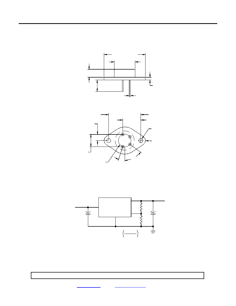
The device is designed to operate without external compensation components. However, the amount of external filtering of these voltage
regulators depends upon the circuit layout. If in a specific application the regulator is more than four inches from the filter capacitor, a 2
µF
solid tantalum capacitor should be used at the input. A 1
µF capacitor should be used at the output to reduce transients created by fast
switching loads, as seen in the basic test circuit. These filter capacitors must be located as close to the regulator as possible.
Caution: Permanent damage can result from forcing the output voltage higher than the input voltage. A protection diode from output to
input should be used if this condition exists.
VOLTAGE OUTPUT
The device has an adjustable output voltage from -2.55 to -24V which can be programmed by the external resistor network (potentiometer
or two fixed resistors) using the relationship:
Example:
If R1 = 0
and R2 = 5k, Then
V
OUT
= V
CONTROL
R1 + R2
V
OUT
= -2.55 V nominal,
R2
or, if R1 = 12.8 k
and R2 = 2.1 k then
V
OUT
= -18V.
Micropac Industries cannot assume any responsibility for any circuits shown or represent that they are free from patent infringement.
Micropac reserves the right to make changes at any time in order to improve design and to supply the best product possible.
MICROPAC INDUSTRIES, INC. HYBRID MICROELECTRONICS PRODUCTS DIVISION
∑ 905 E. Walnut St., Garland, TX 75040 ∑ (972) 272-3571 ∑ Fax (972) 494-2281
www.micropac.com
E-MAIL:
hybridsales@micropac.com
12/12/01
3
52149/52174
NEGATIVE ADJUSTABLE 5-AMP, VOLTAGE REGULATOR
Mechanical Configuration
Note: All Dimension in notes and Millimeters (parenthesis)
R .177 (4.5)
PIN 3
54∞
12∞
PIN 4
PIN 2
PIN 1
0.47 (11.34)
DIA. PIN CIRCLE
.440 (11.16)
.420 (10.57)
.205 (5.21)
.225 (5.71)
1.177 (29.30)
1.197 (30.40)
.675 (17.14)
.655 (16.64)
ÿ.151 (3.84)
ÿ.161 (4.09)
2 HOLES
.041 (1.04)
.037 (0.94)
DIA.
.067 (1.70)
MAX.
SEATING PLANE
.421 (10.69)
MIN.
.293 (7.44)
.273 (6.90)
1.551 (39.40)
1.531 (38.19)
MAX.
.770 (19.56)
R1
R2
4
3
2
1
C >1.0uF
L
IN
V
C =2uF
IN
SOLID
TANTALUM
OUT
V
+
+
OUT
V =VCONT
R1+R2
R2
Basic Test Circuit Adjustable Output Voltage