 | –≠–ª–µ–∫—Ç—Ä–æ–Ω–Ω—ã–π –∫–æ–º–ø–æ–Ω–µ–Ω—Ç: 53259 | –°–∫–∞—á–∞—Ç—å:  PDF PDF  ZIP ZIP |

Micropac Industries cannot assume any responsibility for any circuits shown or represent that they are free from patent infringement.
Micropac reserves the right to make changes at any time in order to improve design and to supply the best product possible.
MICROPAC INDUSTRIES, INC.
MICROCIRCUITS DIVISION ∑ 905 E. Walnut St., Garland, TX 75040 ∑ (972) 272-3571 ∑ Fax (972) 494-2281
www.micropac.com
E-MAIL: hybridsales@micropac.com 7/29/02
Pg. 1 of 6
53259
POWER MOSFET OPTOCOUPLER
400V / 50 HERMETICALLY SEALED
Mii
MICROCIRCUITS DIVISION
Features:
∑ Hermetically Sealed 8-Pin Dual-In-Line
package
∑ Normally Closed Contact
∑ Performance over ≠55∞C to +125∞C Ambient
Temperature Range
∑ ±400 VDC Blocking Voltage in Bi-directional
Mode
∑ AC/DC Switching
∑ Maximum AC / DC Load Current: 0.12 A / 0.24 A
∑ 1500 VDC Withstand Test Voltage
∑ Optically Isolated
∑ 1.5 A Output Surge Current
∑ Same foot print as HSSR 7111 / Mii 53111
Applications:
∑ Satellite / Space Systems
∑ Military / High Reliability Systems
∑ Power Distribution Control
∑ AC/DC Electromechanical or Reed Relay
Replacement
∑ I/O Modules for Automated Test Equipment
∑ Process Control
∑ Telecom Applications
∑ Medical Electronics
DESCRIPTION
The 53259 is a single channel power MOSFET optocoupler. Low on-resistance of the MOSFET outputs, combined
with 1500 VDC isolation between input and output, makes this optocoupler ideal for many solid state relay
applications. Operation is specified over the full military temperature range. The part is supplied in an eight-pin,
dual-in-line ceramic package, available in variety of quality levels from COTS to class K including any custom
screening requirements. The basic data sheet part is environmentally screened to H level in accordance with Table
C-IX of MIL-PRF-38534. For ordering part number; consult with Micropac factory for detail. The part is normally
shipped with gold plated leads, but lead finishes per MIL-PRF-38534 are available.
Functionally, the device operates as a single-pole, normally closed (1 Form B) solid state relay. The device is
actuated by an input current, which can be supplied from standard logic types such as open-collector TTL. The
input current biases a light emitting diode that is optically coupled to an integrated photovoltaic diode array. The
photovoltaic array powers control circuitry that operates the output MOSFETs.
Optimum switching of either AC or DC loads is provided by a configurable output. For AC loads, connection A in
Figure 1 must be used. Connection A will also switch DC loads but connection B, in Figure 1, provides DC-only
operation with the advantages of substantial reduction in on-resistance and twice the output current capability as
that obtained with connection A.

Micropac Industries cannot assume any responsibility for any circuits shown or represent that they are free from patent infringement.
Micropac reserves the right to make changes at any time in order to improve design and to supply the best product possible.
MICROPAC INDUSTRIES, INC.
MICROCIRCUITS DIVISION ∑ 905 E. Walnut St., Garland, TX 75040 ∑ (972) 272-3571 ∑ Fax (972) 494-2281
www.micropac.com
E-MAIL: hybridsales@micropac.com 7/29/02
Pg. 2 of 6
53259 Power MOSFET Optocoupler
___________________________________________________________________________________________
ABSOLUTE MAXIMUM RATINGS
Storage Temperature Range ..................................................................................................................-65∞C to +150∞C
Operating Ambient Temperature - T
A
.....................................................................................................-55∞C to +125∞C
Junction Temperature - T
J
........................................................................................................................................150∞C
Lead Solder Temperature (1.6mm below seating plane for 10 seconds) ............................................................260
∞C
Average Input Current - I
F
........................................................................................................................................20 mA
Peak Repetitive Input Current - I
Fpk
(Pulse Width < 100ms; duty cycle < 50%) ..................................................40 mA
Peak Surge Input Current - I
FPK
surge (Pulse Width < 0.2ms; duty cycle < 0.1%) ..........................................100 mA
Reverse Input Voltage - V
R
....................................................................................................................................5 V
Output Current
Connection A ≠ I
O
..........................................................................................................................................0.12 A
Connection B - I
O
..........................................................................................................................................0.24 A
Inrush Output Current
Connection A - I
Opk
surge ... ...........................................................................................................................1.5 A
Output Blocking Voltage
Connection A - V
O
..................................................................................................................................± 400 VDC
Connection B - V
O
........................................................................................................................ 0 V to +400 VDC
Output Power Dissipation ..............................................................................................................................500 mW
RECOMMENDED OPERATING CONDITIONS:
PARAMETER SYMBOL
MIN
MAX
UNITS
Input Current (off)
I
F (OFF)
5 20
mA
Input Voltage (on)
V
F (ON)
0 0.6
VDC
Operating Temperature
T
A
-55 +125 ∞C
Note: On state means contact closed. Off state means contact open.

Micropac Industries cannot assume any responsibility for any circuits shown or represent that they are free from patent infringement.
Micropac reserves the right to make changes at any time in order to improve design and to supply the best product possible.
MICROPAC INDUSTRIES, INC.
MICROCIRCUITS DIVISION ∑ 905 E. Walnut St., Garland, TX 75040 ∑ (972) 272-3571 ∑ Fax (972) 494-2281
www.micropac.com
E-MAIL: hybridsales@micropac.com 7/29/02
Pg. 3 of 6
53259 Power MOSFET Optocoupler
___________________________________________________________________________________________
ELECTRICAL SPECIFICATIONS
T
A
= -55
∞C to +125∞C, unless otherwise specified.
Parameter Sym.
Min.
Typ.*
Max.
Units
Test
Conditions
Notes
Output Blocking Voltage
V
O(OFF)
400 ---- ---- V
I
F
= 10 mA
I
O
= 10
µA
Output On-Resistance
(Connection A)
---- 25 50
I
F
= 0 mA
I
O
= 120 mA
(pulse duration
30 ms)
2
Figure
3
Output On-Resistance
(Connection B)
R
(ON)
---- 12 25
I
F
= 0 mA
I
O
= 240 mA
(pulse duration
30 ms)
Output Leakage Current
I
O (OFF)
---- 0.2 10
µA
V
O(OFF)
= 400 V
Input Forward Voltage
V
F
1.0 1.2 1.9 V I
F
= 10 mA
Input Reverse
Breakdown Voltage
V
R
5.0 12 ---- V
I
R
= 10
µA
Input-Output Insulation
I
I-O
---- ---- 1.0
µA
RH
45%, t = 5 s
V
I-O
= 1500 VDC
T
A
= 25
∞C
3, 4
Turn-On Time
t
ON
---- 0.3 3.0 ms
I
F
= 0 mA
I
O
= 120 mA
Figure
3
Turn-Off time
t
OFF
---- 0.1 1.0 ms
I
F
= 10 mA
I
O
= 120 mA
Figure
3
* All typical values are at T
A
= 25∫C, unless otherwise specified.
Notes:
1. Maximum junction to case thermal resistance (
JC
) for the device is 15∫C/W, where case temperature (T
C
), is
measured at the center of the package bottom.
2. During the pulsed R
(ON)
measurement (I
O
duration < 30 ms), ambient (T
A
) and case temperature (T
C
) are equal.
3. Pins 2 through 3 shorted together and pins 5 through 8 shorted together.
4. This is a momentary withstand test, not an operating condition.
5. Care should be taken not to exceed the maximum output power dissipation, maximum case temperature, and
maximum junction temperature when repetitively switching loads.
Micropac Industries cannot assume any responsibility for any circuits shown or represent that they are free from patent infringement.
Micropac reserves the right to make changes at any time in order to improve design and to supply the best product possible.
MICROPAC INDUSTRIES, INC.
MICROCIRCUITS DIVISION ∑ 905 E. Walnut St., Garland, TX 75040 ∑ (972) 272-3571 ∑ Fax (972) 494-2281
www.micropac.com
E-MAIL: hybridsales@micropac.com 7/29/02
Pg. 4 of 6
53259 Power MOSFET Optocoupler
___________________________________________________________________________________________
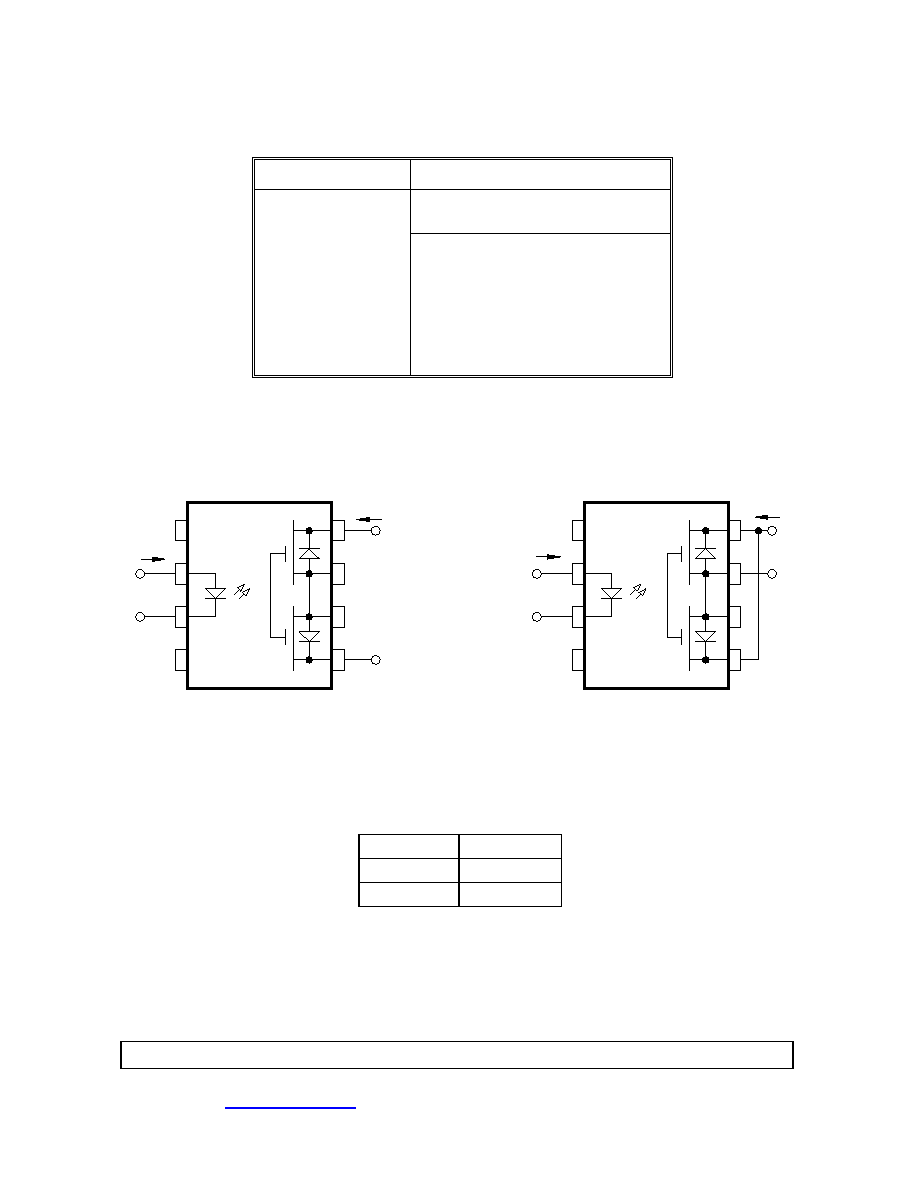
CONNECTION A
AC/DC CONNECTION
4
F
-
+
3
2
1
-
5
4
5
CONNECTION B
DC CONNECTION
Terminal number Terminal symbol
Connection A Conneciton B
(AC or DC load) (DC load only)
+
6
7
8
NC = No connection
-
+
3
2
1
6
7
8
+
-
I
F
V
O
I
O
V
F
I
F
V
VO
O
I
8
6
7
3
5
4
2
1
V
NC
V
NC
V
NC
NC
V
F-
O+
O-
F+
F-
V
VO+
O-
V
V O+
NC
NC
V F+
V O-
Figure 1. Terminal Connections
INPUT OUTPUT
OFF ON
ON OFF
Figure 2. True Table
Micropac Industries cannot assume any responsibility for any circuits shown or represent that they are free from patent infringement.
Micropac reserves the right to make changes at any time in order to improve design and to supply the best product possible.
MICROPAC INDUSTRIES, INC.
MICROCIRCUITS DIVISION ∑ 905 E. Walnut St., Garland, TX 75040 ∑ (972) 272-3571 ∑ Fax (972) 494-2281
www.micropac.com
E-MAIL: hybridsales@micropac.com 7/29/02
Pg. 5 of 6
53259 Power MOSFET Optocoupler
________________________________________________________________________________________
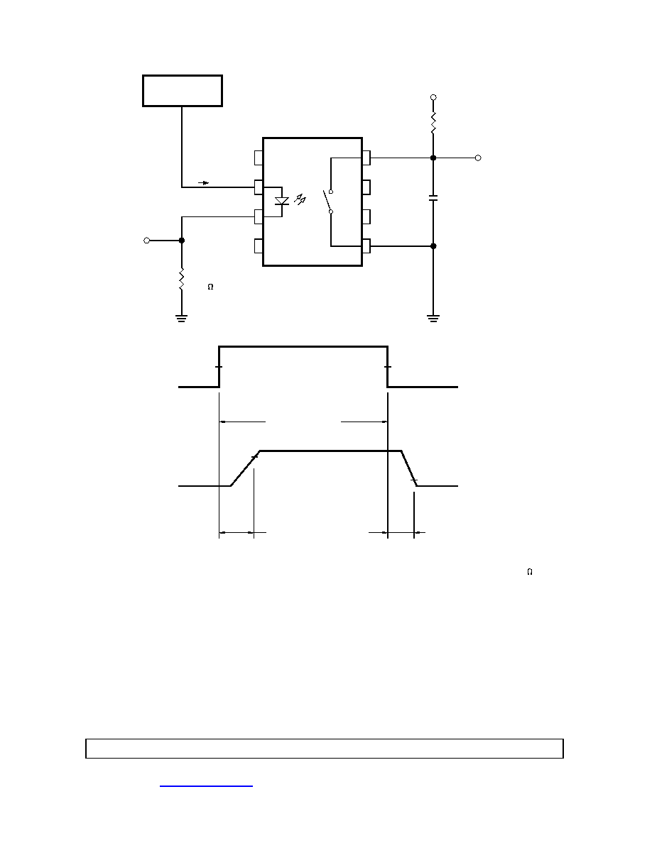
PULSE GEN
(SEE NOTE 1)
50%
200
NOTES:
1. PULSE GENERATOR HAS THE FOLLOWING CHARACTERISTICS: OUTPUT IMPEDANCE = 50
AND t
= t
= 5.0 ns.
2. LOAD CAPACITANCE (C
) INCLUDES PROBE AND JIG CAPACITANCE.
r f
GND
MONITOR
I
90%
ON
t
10%
OFF
MONITOR
NODE
+
PULSE
WIDTH
= 15 ms
V
-
4
3
GND
50%
5
6
= 25 pF
(SEE NOTE 2)
2
1
7
8
R
V
F
F
M
R
L
VO
C L
DD
F
I
F
I
O
V
t
L
Figure 3. Switching Test Circuit and Waveform.