MICROPAC INDUSTRIES, INC.
OPTOELECTRONIC PRODUCTS DIVISION ∑ 725 E. Walnut St., Garland, TX 75040 ∑ (972) 272-3571 ∑ Fax (972) 487-6918
www.micropac.com
E-MAIL: optosales@micropac.com
6 - 6
61053
SILICON PHOTOTRANSISTOR "PIGTAIL"
(TYPE GS3020)
Mii
OPTOELECTRONIC PRODUCTS
DIVISION
Features:
∑ Hermetically
sealed
∑ High
sensitivity
∑ Pigtail version available
∑ Suitable for high-density pc board mounting
∑ Spectrally matched to the 62017 Series LED.
Applications:
∑ Incremental
encoding
∑ Reflective
sensors
∑ Position
sensors
∑ Level
sensors
DESCRIPTION
The 61053 is an N-P-N Planar Silicon phototransistor in a package designed to be mounted in a double-clad printed circuit
board. It is available in a range of sensitivities and is lensed for minimum response to stray light. High sensitivity, low dark
current leakage, and low saturation voltage make this device ideal for interfacing with TTL circuits. This sensor is also
available with a lead attached to the case so that it may be connected without the use of printed circuit boards. Available
custom binned to customer specifications or screened to MIL-PRF-19500.
ABSOLUTE MAXIMUM RATINGS
Storage Temperature..........................................................................................................................................-65∞C to +150∞C
Operating Temperature (See part selection guide for actual operating temperature) ......................................-65∞C to +125∞C
Collector-Emitter Voltage........................................................................................................................................................50V
Emitter-Collector Voltage.......................................................................................................................................................... 7V
Power Dissipation (Derate at the rate of 0.5 mW/
∞
C above 25∞C) ...................................................................................50mW
Lead Soldering Temperature (3 minutes) ......................................................................................................................... 240
∞
C
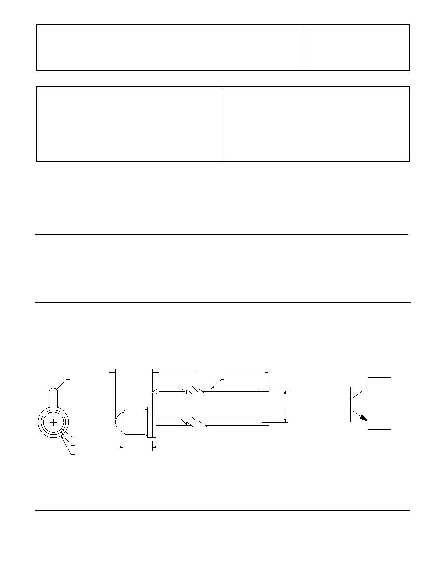
Package Dimensions Schematic Diagram
ÿ.025 [0.64]
0.114 [2.90]
0.100 [2.54]
0.089 [2.26]
OPTIONAL
ALL DIMENSIONS ARE IN INCHES [MILLIMETERS]
ÿ0.095 [ÿ2.41]
ÿ0.063 [ÿ1.60]
ÿ0.077 [ÿ1.96]
1.000 [25.40]
C
E
E
C
MICROPAC INDUSTRIES, INC.
OPTOELECTRONIC PRODUCTS DIVISION ∑ 725 E. Walnut St., Garland, TX 75040 ∑ (972) 272-3571 ∑ Fax (972) 487-6918
www.micropac.com
E-MAIL: optosales@micropac.com
6 - 7
61053
SILICON PHOTOTRANSISTOR "PIGTAIL" (TYPE GS3020)
ELECTRICAL CHARACTERISTICS
T
A
= 25∞C unless otherwise specified.
PARAMETER
SYMBOL
MIN
TYP
MAX
UNITS
TEST CONDITIONS
NOTE
Light Current
61053-X01
61053-X02
61053-X03
61053-X04
I
L
0.7
1.5
3.0
6.0
2.0
4.0
7.0
--
mA
V
CE
= 5.0V, H = 5 mW/cm
2
1
Dark Current
61053-XXX
I
D
25
nA
V
CE
= 30V, H = 0
Collector-Emitter Breakdown Voltage 61053-XXX
BV
CEO
50
V
I
C
= 100
µ
A
Emitter-Collector Breakdown Voltage 61053-XXX
BV
ECO
7
V
I
E
= 100
µ
A
Light Current Rise Time 61053-X01
61053-X02
61053-X03
61053-X04
t
r
2.0
3.0
5.0
7.0
R
L
= 1K
, V
CC
= 5V,
I
L
= 1.0mA
Saturation Voltage 61053-X01
V
CE (sat)
0.3
V
I
C
= 0.4mA, H = 5 mW/cm
2
Angular Response 61053-X01
12
degrees
2
NOTES:
1.
Irradiance in mW/cm
2
from a tungsten source at a color temperature of 2870K..
2.
The angle between incidence for peak response and incidence for 50% of peak response.
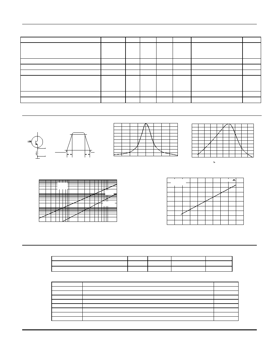
ANGULAR RESPONSE
RELATIVE SPECTRAL RESPONSE
H
PULSE RESPONSE TEST
CIRCUIT AND WAVEFORM
DUT
RL
OUTPUT
Vcc
IL
tr
tf
10%
90%
A N G L E [ D E G R E E S ]
- 3 0
- 2 0
- 1 0
0
2 0
3 0
1 0
0
2 0
4 0
6 0
1 0 0
R
E
L
A
T
I
VE
R
ESP
O
N
SE
[
%
8 0
4 0
- 4 0
WAVELENGTH [um]
0.4
0.5
0.6
0.7
0.9
1.0
0.8
0
20
40
60
100
R
E
L
A
TI
VE R
ESPO
N
SE [
%
]
80
1.1
0.3
0.2
1.2
10
30
50
70
90
NORMALIZED LIGHT CURRENT
versus RADIATION FLUX DENSITY
0.5
0.2
1.0
0.1
0.01
L
.
L
I
GH
T
CU
RRENT
[
N
ORM
A
L
I
Z
E
D
I
N. RADIATION FLUX DENSITY [mW/cm 2]
T
O
2
0
m
W
/
c
m
2
T
UNGS
T
EN
SOURCE]
1.0
10
10
20
5.0
20
V =50 V
T =25∞C
J
CC
TUNGSTEN
SOURCE
GaAs
SOURCE
NORMALIZED LIGHT CURRENT
versus TEMPERATURE
T AMBIENT TEMPERATURE [∞C]
-100
-75
-25
-50
0
0.2
0.4
0.6
1.0
I
[N
O
R
M
A
LIZ
E
D
]
0.8
L
A
1.2
1.6
1.4
2.0
1.8
0
25
50
75
150
125
100
Vcc = 5.0 V
NOTE 1
R =100
L
RECOMMENDED OPERATING CONDITIONS:
PARAMETER
SYMBOL
MIN
MAX
UNITS
Bias Voltage-Collector/Emitter
I
F
5
10
mA
Irradiance (H)
H
15
25
mW/cm
2
SELECTION GUIDE
PART NUMBER
PART DESCRIPTION
I
L
Range
61053-001
Silicon Phototransistor in coax package, commercial version
0.7 to 2mA
66153-101
Silicon Phototransistor in coax package (-55
∞
to +100
∞
C) with 100% screening
0.7 to 2mA
61053-002
Silicon Phototransistor in pill package, commercial version
1.5 to 4mA
61053-102
Silicon Phototransistor in pill package (-55
∞
to +100
∞
C) with 100% screening
1.5 to 4mA
61053-003
Silicon Phototransistor in pill package, commercial version
3 to 7mA
61053-103
Silicon Phototransistor in pill package (-55
∞
to +100
∞
C) with 100% screening
3 to 7mA
61053-004
Silicon Phototransistor in pill package, commercial version
6+mA
61053-104
Silicon Phototransistor in pill package (-55
∞
to +100
∞
C) with 100% screening
6+mA
NOTE: Add L following dash number ( e.g. -004L ) to indicate loop lead.