
MICROPAC INDUSTRIES, INC.
OPTOELECTRONIC PRODUCTS DIVISION ∑ 725 E. Walnut St., Garland, TX 75040 ∑ (972) 272-3571 ∑ Fax (972) 487-6918
www.micropac.com
E-MAIL: optosales@micropac.com
5 - 2
66053
SINGLE-CHANNEL, LOW-INPUT CURRENT
LEADLESS CHIP CARRIER OPTOCOUPLER
Mii
OPTOELECTRONIC PRODUCTS
DIVISION
REVISION 9/28/00
Features:
∑ Electrically similar to 6N140
∑ Hermetically sealed 24 Pin LCC
∑ High Current Transfer ratio: 1000% typical
∑ CTR and 1
OH
guaranteed over 55∞C to + 125∞C
∑ ambient temperature range
∑ Standard and high reliability screened parts
available
∑
1000 Vdc isolation test voltage
∑
Low input current requirement: 0.5mA
∑
Low output saturation voltage: 0.1V typical
∑
Low power consumption
∑
Leadless chip carrier package
∑ Faraday shield provides high common mode
rejection
DESCRIPTION
The 66053 optocoupler contains an infrared LED optically
coupled to a corresponding high gain darlington detector.
This unique optocoupler provides high CTR and low
leakage current over the full military temperature range (-
55∞C to + 125∞C). The 66053 is a 24 pin hermetically
sealed leadless chip carrier and is available in standard
and screened versions or tested to customer specifications.
RECOMMENDED OPERATING CONDITIONS
PARAMETER
SYMBOL
MIN
MAX
UNITS
Input Current, Low
Level Each Channel
IFL
2
µA
Input Current, High
Level Each Channel
IFH
0.5
5
mA
Supply Voltage
VCC
2.0
18
V
ABSOLUTE MAXIMUM RATINGS
Output current - I
O ...........................................................................................................................................................................................................................................................................
40mA
Output voltage - V
O
..................................................................................................................................................... -0.5 to 20V (1)
Supply voltage - V
CC
................................................................................................................................................... -0.5 to 20V (1)
Output power dissipation ..................................................................................................................................................50 mW (2)
Storage temperature ............................................................................................................................................... -65∞C to +150∞C
Operating temperature............................................................................................................................................. -55∞C to +125∞C
Lead solder temperature ........................................................................................................................................260∞C for 10 sec.
Peak input current (<1ms duration) ......................................................................................................................................... 20mA
Reverse input voltage - V
R
............................................................................................................................................................. 5V
Average input current - I
F
.....................................................................................................................................................10mA (3)
Notes:
1.
The lowest total I
OH
over temperature is developed by keeping V
CC
as low as possible, but greater than 2.0 volts. The negative voltage at the
detector side should be applied to PIN 10.
2.
Collector output power plus one fourth of the total supply power is total output power. Derate at 0.46mW/∞C above 25∞C.
3. Derate
I
F
at 0.05mA /∞C above 25∞C.
Package Dimensions Schematic Diagram
NO. 1 LEAD
Mii 66053
XXXXX
0.008
K
1
A
2
GND
Vo
Vcc
10
14
15
IDENTIFIER
[10.160 +.254,-.127]
[1.778]
[1.270]
[.203]
[.889]
REF.
RAD,TYP
0.020
(.508)
[1.143]
0.045
0.070
0.050
0.035
0.400+.010,-.055
MICROPAC INDUSTRIES, INC.
OPTOELECTRONIC PRODUCTS DIVISION ∑ 725 E. Walnut St., Garland, TX 75040 ∑ (972) 272-3571 ∑ Fax (972) 487-6918
www.micropac.com
E-MAIL: optosales@micropac.com
5 - 3
66053
SINGLE≠CHANNEL, LOW-INPUT CURRENT, LEADLESS CHIP CARRIER OPTOCOUPLER, Continued
REVISION A 9/28/00
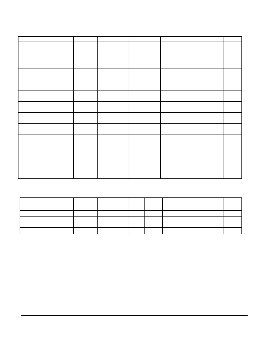
ELECTRICAL CHARACTERISTICS
(T
A
= -55
∞C to 125∞C) unless otherwise specified
PARAMETER
SYMBOL
MIN
TYP**
MAX
UNITS
TEST CONDITIONS
NOTE
Current Transfer Ratio
CTR
300
300
200
1000
750
400
%
%
%
I
F
= 0.5mA, V
O
= 0.4V, V
CC
= 4.5V
I
F
= 1.6mA, V
O
= 0.4V, V
CC
= 4.5V
I
F
= 5.0mA, V
O
= 0.4V, V
CC
= 4.5V
1
Logic Low Output Voltage
V
OL
0.1
0.2
0.4
0.4
V
V
I
F
= 0.5mA, I
OL
= 1.5mA, V
CC
= 4.5V
I
F
= 5.0mA, I
OL
= 10mA, V
CC
= 4.5V
Logic High Output Current
I
OH
.005
250
µ
A
I
F
= 2
µ
A
V
O
= V
CC
= 18V
Logic Low Supply Current
I
CCL
2
4
mA
I
F
= 1.6mA
V
CC
= 18V
Logic High Supply Current
I
CCH
.010
40
µ
A
I
F
=
0
V
CC
= 18V
Input Forward Voltage
V
F
1.4
1.8
V
I
F
= 1.6mA, T
A
= 25∞C
Input Reverse Breakdown Voltage
BV
R
5
V
I
R
= 10µA, T
A
= 25∞C
Input-Output Insulation Leakage
Current
I
I--O
1.0
µA
45% Relative Humidity, T
A
= 25∞C,
t = 5s., V
I-0
= 1000Vdc
2
Propagation Delay Time To Logic
High at Output
t
PLH
6
4
60
30
µ
s
µ
s
I
F
= 0.5mA, R
L
= 4.7k
, V
CC
= 5.0V,
I
F
= 5mA, R
L
= 680
,
V
CC
= 5.0V,
Propagation Delay Time To Logic
Low at Output
t
PHL
8
2
100
10
µ
s
µ
s
I
F
= 0.5mA, R
L
= 4.7k
,
V
CC
= 5.0V,
I
F
= 5mA, R
L
= 680
,
V
CC
= 5.0V,
Common Mode Transient
Immunity at High Output
CM
H
500
1000
V/
µ
s
I
F
= OmA, R
L
= 1.5k
,
V
CM
= 50V
P-P
,
V
CC
= 5.0V, T
a
= 25∞C
3
Common Mode Transient
Immunity at Low Output
CM
L
500
1000
V/
µ
s
I
F
= 1.6mA, R
L
= 1.5k
,
V
CM
= 50V
P-P
,
V
CC
= 5.0V, T
a
= 25∞C
4
**All typical values are at VCC
=
5VA
= 25∞C
TYPICAL CHARACTERISTICS
T
A
= 25
∞C, V
CC
= 5V Each Channel
PARAMETER
SYMBOL
MIN
TYP
MAX
UNITS
TEST CONDITIONS
NOTE
Resistance (Input-Output)
R
I-0
10
12
V
I--O
= 500Vdc, T
A
= 25
∞
C
2
Capacitance (Input-Output)
C
I-0
1.5
pF
f = 1MHz, T
A
= 25
∞
C
2
Temperature Coefficient
Of Forward Voltage
v
F
T
A
-1.8
mV/
∞
C
I
F
= 1.6mA
Input Capacitance
C
IN
60
pF
f = 1MHz, V
F
= 0, T
A
= 25
∞
C
NOTES:
1.
CURRENT TRANSFER RATIO is defined as the ratio of output
collector current, I
O
, to the forward LED input current, I
F
, times
100%.
2.
Device considered a two-terminal device. Pins 1 and 2 are shorted
together and pins 10, 14, and 15 are shorted together.
3. CM
H
is the maximum tolerable common mode transient to assure
that the output will remain in a high logic state (i.e. V
O
> 2
.0V).
4. CM
L
is the maximum tolerable common mode transient to assure
that the output will remain in low logic state (i.e. V
O
<
0.8V).