MICROPAC INDUSTRIES, INC.
OPTOELECTRONIC PRODUCTS DIVISION ∑ 725 E. Walnut St., Garland, TX 75040 ∑ (972) 272-3571 ∑ Fax (972) 487-6918
www.micropac.com
E-MAIL: optosales@micropac.com
5 - 6
66064
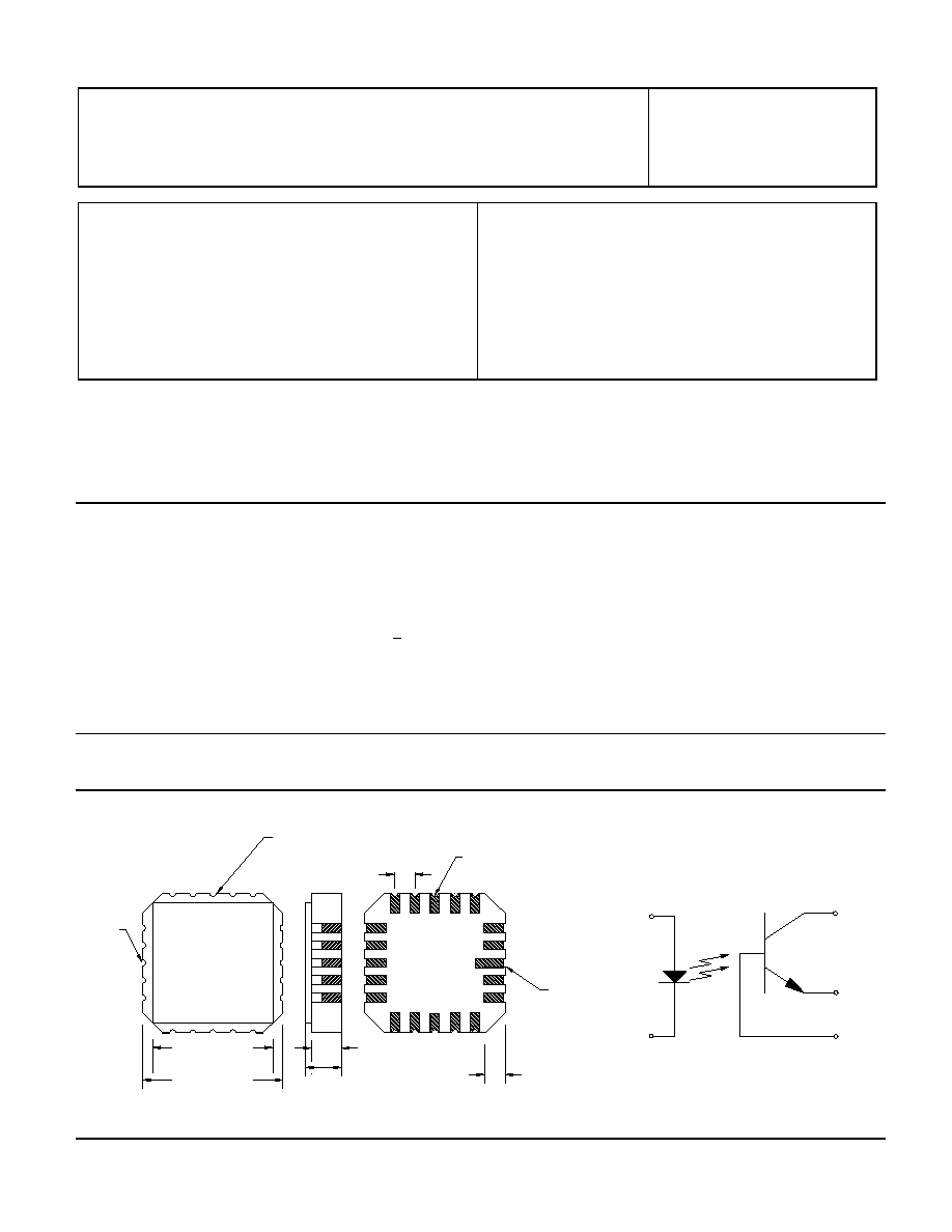
SINGLE CHANNEL, HERMETIC 20 PIN LCC,
ELECTRICALLY SIMILAR TO 4N47, 4N48, 4N49
Mii
OPTOELECTRONIC PRODUCTS
DIVISION
Features:
∑ High
Reliability
∑ Base lead provided for conventional transistor
biasing
∑ Very high gain, high voltage transistor
∑ Stability over wide temperature range.
∑ +1kV electrical isolation
Applications:
∑ Eliminate ground loops
∑ Level
shifting
∑ Line
receiver
∑ Switching power supplies
∑ Motor
control
DESCRIPTION
The 66064 single channel optocoupler consists of an LED optically coupled to a high gain silicon phototransistor in a 20 pin
LCC package. The 66064 is electrically equivalent to the 4N47 (-X01), 4N48 (-X02) and the 4N49 (-X03) and is available in
standard and screened versions.
ABSOLUTE MAXIMUM RATINGS
Collector-Base Voltage .............................................................................................................................................................50V
Collector-Emitter Voltage (Value applies to emitter-base open-circuited & the input-diode equal to zero) ...........................50V
Emitter-Base Voltage..................................................................................................................................................................7V
Reverse Input Voltage ...............................................................................................................................................................6V
Input Diode Continuous Forward Current at (or below) 65∞C Free-Air Temperature (see note 1) .....................................40mA
Peak Forward Input Current (Value applies for tw
<
1
µ
s, PRR
<
300 pps) ...............................................................................1A
Continuous Collector Current ................................................................................................................................................50mA
Continuous Transistor Power Dissipation at (or below) 25∞C Free-Air Temperature (see Note 2) .................................300mW
Storage Temperature.......................................................................................................................................... -65∞C to +150∞C
Operating Free-Air Temperature Range ............................................................................................................. -55∞C to +125∞C
Lead Solder Temperature (10 seconds max.) .................................................................................................................... 260∞C
Notes:
1. Derate linearly to 125∞C free-air temperature at the rate of 0.67 mA/∞C above 65∞C.
2. Derate linearly to 125∞C free-air temperature at the rate of 2 mW/∞C.
Package Dimensions Schematic Diagram
A
K
20
2
12
10
C
E
ALL DIMENSIONS ARE IN INCHES [MILLIMETERS]
0.3000 [7.62]
0.3500 [8.89]
0.008 [R0.20] TYP.
B
11
TYP 0.0500 [1.27]
0.0500 [1.27] TYP
0.0750 [1.91]
0.0900 [2.29]
PIN 1
PIN 1
PIN 16
MICROPAC INDUSTRIES, INC.
OPTOELECTRONIC PRODUCTS DIVISION ∑ 725 E. Walnut St., Garland, TX 75040 ∑ (972) 272-3571 ∑ Fax (972) 487-6918
www.micropac.com
E-MAIL: optosales@micropac.com
5 - 7
66064
SINGLE CHANNEL, 20 PIN LCC, EQUIVALENT TO 4N47, 4N48, 4N49
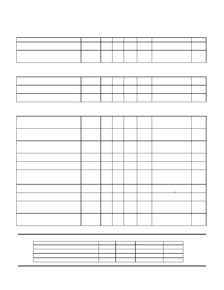
ELECTRICAL CHARACTERISTICS
T
A
= 25
∞C unless otherwise specified.
PARAMETER
SYMBOL
MIN
TYP
MAX
UNITS
TEST CONDITIONS
NOTE
Input Diode Static Reverse Current
I
R
100
µA
V
R
= 2V
Input Diode Static Forward Voltage
-55
∞
C
+25
∞
C
+100
∞
C
V
F
1
0.8
0.7
1.7
1.4
1.3
V
V
V
I
F
= 10mA
OUTPUT TRANSISTOR
T
A
= 25
∞C unless otherwise specified.
Collector-Base Breakdown Voltage
V
(BR)CBO
45
V
I
C
= 100
µ
A, I
B
= 0, I
F
= 0
Collector-Emitter Breakdown Voltage
V
(BR)CEO
40
V
I
C
= 1mA, I
B
= 0, I
F
= 0
Emitter-Base Breakdown Voltage
V
(BR)EBO
7
V
I
C
= 0mA, I
E
= 100
µ
A, I
F
= 0
COUPLED CHARACTERISTICS
T
A
= 25
∞C unless otherwise specified.
On State Collector Current
-X01
T
a
= +25
∞
C
-X02
-X03
I
C(ON)
0.5
1
2
-
5
10
mA
V
CE
= 5V, I
B
= 0, I
F
= 1mA
On State Collector Current
-X01
T
a
= -55
∞
C
-X02
-X03
I
C(ON)
0.7
1.4
2.8
mA
V
CE
= 5V, I
B
= 0, I
F
= 2mA
On State Collector Current
-X01
T
a
= +125
∞
C
-X02
-X03
I
C(ON)
0.5
1.0
2.0
mA
V
CE
= 5V, I
B
= 0, I
F
= 2mA
Off State Collector Current
I
C(OFF)
100
nA
V
CE
= 20V, I
B
= 0, I
F
= 0mA
Off State Collector Current, T
a
= 100
∞
C
I
C(OFF)
100
µ
A
V
CE
= 20V, I
B
= 0, I
F
= 0mA
Collector-Emitter Saturation Voltage -X01
-X02
-X03
V
CE(SAT)
V
CE(SAT)
V
CE(SAT)
0.3
0.3
0.3
V
V
V
I
F
= 2mA, I
C
= 0.5mA, I
B
= 0
I
F
= 2mA, I
C
= 1mA, I
B
= 0
I
F
= 2mA, I
C
= 2mA, I
B
= 0
Input to Output Resistance
R
IO
10
11
V
IN-OUT
= 1kV, t
w
= 100
µ
s,
duty cycle
<
1%
1
Input to Output Capacitance
C
IO
2.5
5
pF
F = 1MHz, V
IN-OUT
= 0
Rise Time (Phototransistor Operation)
-X01
or
-X02
Fall Time -X03
t
r
or
t
f
10
10
10
20
25
25
µ
s
V
CE
= 10V, I
B
= 0, I
F
= 5mA,
R
L
= 100
Rise Time (Photodiode Operation) -X01
or -X02
Fall Time
-X03
t
r
or
t
f
0.85
0.85
0.85
3
3
3
µ
s
V
CE
= 10V, I
E
= 0, I
F
= 5mA,
R
L
= 100
NOTES:
1.
These parameters are measured between all phototransistor leads shorted together and with both input diode leads shorted together.
RECOMMENDED OPERATING CONDITIONS:
PARAMETER
SYMBOL
MIN
MAX
UNITS
Input Current, Low Level
I
FL
0
100
µ
A
Input Current, High Level
I
FH
1
2
mA
Supply Voltage
V
CC
5.0
20
V
Operating Temperature
T
A
-55
125
∞
C