MICROPAC INDUSTRIES, INC.
OPTOELECTRONIC PRODUCTS DIVISION ∑ 725 E. Walnut St., Garland, TX 75040 ∑ (972) 272-3571 ∑ Fax (972) 487-6918
www.micropac.com
E-MAIL: optosales@micropac.com
3 - 38
66079
OPTICALLY COUPLED DIGITAL FILTER
Mii
OPTOELECTRONIC PRODUCTS
DIVISION
Features:
∑ DSCC Approved 916761HXX
∑ 10 MBd typical
∑ Meets Tempest EMI/RFI emanation criteria
∑ TTL compatible input and output
∑ RFI Rejection 80dB to 1GHz
∑
Faraday shield to provide high common mode
rejection
Applications:
∑ Military and space
∑ Secure communication systems
∑ Isolated receiver input
∑ Microprocessor system interface
∑ Digital isolation for A/D, D/A converters
DESCRIPTION
The 66079 Optically Coupled Digital Filter consists of an LED optically coupled to a high speed, high gain inverting detector
gate. Maximum isolation can be achieved while providing a TTL output capable of switching with propagation delays of 55nS
typical. The 66079 is a hermetically sealed package which is threaded in order to provide convenient bulkhead mounting and
is available in standard and screened versions or tested to customer specifications. The 66079-001 is a hermetically sealed
package which can be soldered or press-fit mounted and is also available in standard and MIL-PRF-38534 screened versions
or tested to customer specifications.
ABSOLUTE MAXIMUM RATINGS
Storage Temperature............................................................................................................................................. -65∞C to +150∞C
Operating Free-Air Temperature Range ............................................................................................................... -55∞C to +125∞C
Lead Solder Temperature........................................................................................... 260
∞
C for 10s (1.6mm below seating plane)
Peak Forward Input Current ..........................................................................................................................40mA (1ms duration)
Forward Input Current Continuous ........................................................................................................................................ 20mA
Supply voltage - V
CC
.................................................................................................................................. 7V(1 minute maximum)
Output Current - I
O
................................................................................................................................................................. 25mA
Output Power Dissipation ...................................................................................................................................................... 40mW
Output Voltage - V
O
.....................................................................................................................................................................7V
Total Power Dissipation ...................................................................................................................................................... 175mW
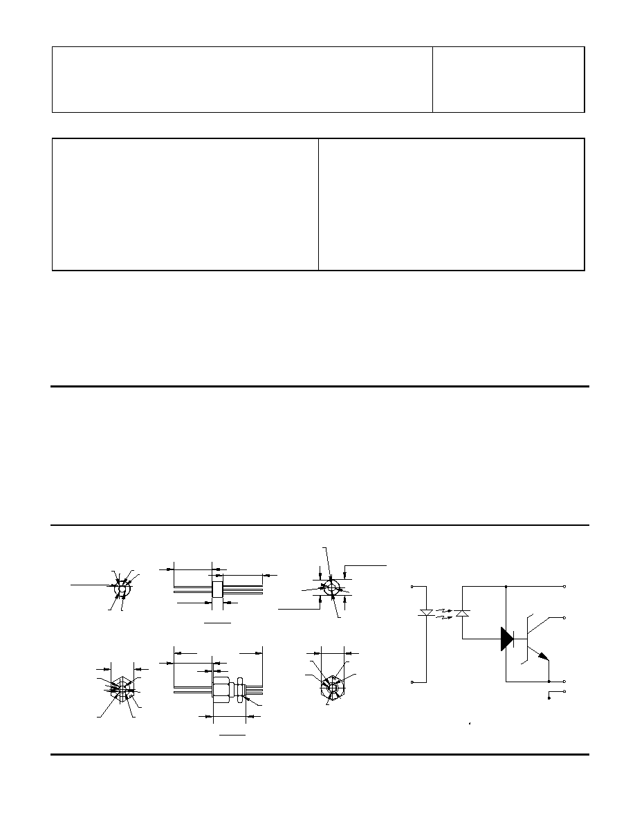
Package Dimensions
Schematic Diagram
OUT
V
.100 ± .005
Vcc
GROUND
NC
ÿ 0.016 [0.406]
0.019 [0.483]
0.221 [5.613]
0.229 [5.817]
0.209 [5.309]
0.212 [5.385]
N.C.
ANODE
CATHODE
0.100 ± .005 [2.540] ÿ
66079-001
ÿ 0.016 [0.406]
0.019 [0.483]
GROUND
N.C.
RED POINT
V OUT
Vcc
0.100ÿ ±.005
0.100ÿ ±.005
RED POINT
N.C.
CATHODE
ANODE
1.230 [31.231]
0.015 [0.381]
MAX
THREADS ARE .250± .010
40 ± 0.1 TURNS PER INCH
66079-000
ALL DIMENSIONS ARE IN INCHES [MILLIMETERS]
ALL DIMENSIONS ARE IN INCHES [MILLIMETERS]
Vcc AND GROUND.
CONNECTED BETWEEN
CAPACITOR MUST BE
A.01 TO 0.1
NOTE:
F BYPASS
GND
OUT
VCC
A
K
CASE
0.532 [13.521]
0.562 [14.283]
0.500 [12.691]
0.560 [14.215]
0.137 [3.480]
0.167 [4.242]
0.312 ±.005
[7.935]
0.500 [12.691]
0.560 [14.215]
0.453 [11.506]
0.463 [11.760]
0.312 ±.005
[7.935]
MICROPAC INDUSTRIES, INC.
OPTOELECTRONIC PRODUCTS DIVISION ∑ 725 E. Walnut St., Garland, TX 75040 ∑ (972) 272-3571 ∑ Fax (972) 487-6918
www.micropac.com
E-MAIL: optosales@micropac.com
3 - 39
66079
OPTICALLY COUPLED DIGITAL FILTER
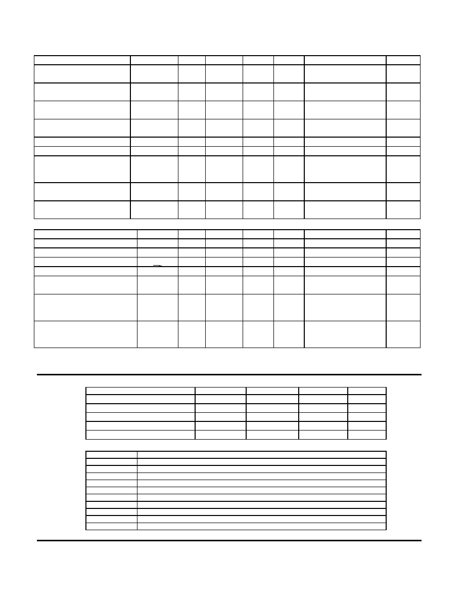
ELECTRICAL CHARACTERISTICS T
a
= -55
∞
C to +125
∞
C unless otherwise specified.
PARAMETER
SYMBOL
MIN
TYP
MAX
UNITS
TEST CONDITIONS
NOTE
High Level Output Current
I
OH
5
250
µA
V
CC
= 5.5V, V
O
= 5.5V,
I
F
= 250µA
Low Level Output Voltage
V
OL
0.5
0.6
V
V
CC
= 5.5V, I
F
= 10mA
I
OL
(Sinking) = 10mA
High Level Supply Current
I
CCH
10
20
mA
V
CC
= 5.5V, I
F
= 0
(Both Channels)
Low Level Supply Current
I
CCL
20
30
mA
V
CC
= 5.5V, I
F
= 20mA
(Both Channels)
Input Forward Voltage
V
F
1.5
1.75
V
I
F
= 20mA
Input Reverse Breakdown Voltage
BV
R
5
V
I
R
= 10µA
Input-Output Insulation Leakage
Current
I
I--O
1.0
µA
V
I--0
= 1500Vdc,
Relative Humidity = 45%
T
a
= 25∞C, t = 5s
Propagation Delay Time To High
Output Level
t
PLH
65
100
ns
R
L
= 510
, C
L
= 15pF.
I
f
= 13mA, t
a
= 25
∞
C
Propagation Delay Time To Low
Output Level
t
PHL
55
100
ns
R
L
= 510
, C
L
= 15pF
I
f
= 13mA, t
a
= 25
∞
C
TYPICAL CHARACTERISTICS
T
a
= 25
∞
C, V
CC
= 5V EACH CHANNEL
PARAMETER
SYMBOL
MIN
TYP
MAX
UNITS
TEST CONDITIONS
NOTE
Input Capacitance
C
IN
60
V
F
= 0, f = MHz
Input to Case Capacitance
C
IC
2
5
pF
V
F
= 0, f = MHz
Input Diode Temperature Coefficient
v
F
-1.9
mV/
∞
C
I
F
= 20mA
Capacitance (Input-Output)
C
I-O
1
3
pF
f = 1MHz
Output Rise-Fall Time (10-90%)
t
f
,
t
f
35
ns
R
L
= 510
, C
L
= 50pF
I
F
= 13mA
Common Mode Transient Immunity
at High Output Level
CM
H
1000
10000
V/
µ
s
V
CM
= 10V (peak),
V
O
(min) = 2V,
R
L
= 510
, I
F
= OmA
1
Common Mode Transient Immunity
at Low Output Level
CM
L
1000
10000
V/
µ
s
V
CM
= 10V (peak),
V
O
(max) = 0.8V,
R
L
= 510
, I
F
= 1OmA
2
NOTES:
1. CM
h
is the max. tolerable common mode transient to assure that the output will remain in a high logic state (i.e. V
O
>
2.0V).
2. CM
l
is the max. tolerable common mode transient to assure that the output will remain in a low logic state (i.e. V
O
<
0.8V).
RECOMMENDED OPERATING CONDITIONS:
PARAMETER
SYMBOL
MIN
MAX
UNITS
Input Current, Low Level Each Channel
I
FL
0
250
µ
A
Input Current, High Level Each Channel
I
FH
12.5
20
mA
Supply Voltage
V
C
4.5
5.5
V
Fan Out (TTL Load) Each Channel
N
6
Operating Temperature
T
A
-55
125
∞
C
SELECTION GUIDE
PART NUMBER
PART DESCRIPTION
66079-000
With housing, with 100% screening
66079-000C
DSCC Drawing # 5962-916761HXX , with housing
66079-001
Without housing, with 100% screening
66079-001C
DSCC Drawing #5962-916760HXX (without housing)
66079-002
With housing, commercial mil-temp (-55
∞
C to +125
∞
C)
66079-003
Without housing, commercial mil-temp (-55
∞
C to +125
∞
C)
66079-004
Without housing, commercial extended temp (-40
∞
C to +80
∞
C)
66079-004H
With housing, commercial extended temp (-40
∞
C to +80
∞
C)
66079-005
Without housing, commercial temp (0
∞
C to +70
∞
C)
66079-005H
With housing, commercial temp (0
∞
C to +70
∞
C)