MICROPAC INDUSTRIES, INC.
OPTOELECTRONIC PRODUCTS DIVISION ∑ 725 E. Walnut St., Garland, TX 75040 ∑ (972) 272-3571 ∑ Fax (972) 487-6918
www.micropac.com
E-MAIL: optosales@micropac.com
5 - 10
66113
SINGLE CHANNEL, SURFACE MOUNT OPTOCOUPLER
Mii
OPTOELECTRONIC PRODUCTS
DIVISION
Features:
∑ Small size saves real estate
∑ Pick and place compatible
∑ Military temperature range
∑ Pin compatible with OPI210 & OPI211
∑ CTR +50% for -X01
∑ CTR +200% for -X02
Applications:
∑ Eliminate
ground
loops
∑ Level
shifting
∑ Line
receiver
∑ Switching power supplies
∑ Motor
control
∑ Pulse transformer replacement
DESCRIPTION
The 66113 is designed to be used where epoxy-based surface mounting is a requirement. State-of-the-art optocoupler
technology is utilized. A high efficiency infrared LED is coupled to a light-sensitive silicon phototransistor. This device is
ideal for automated assembly in pick-and-place applications.
ABSOLUTE MAXIMUM RATINGS
Input to Output Isolation Voltage .................................................................................................................................+1kVdc
Collector-Emitter Voltage (Value applies to emitter-base open-circuited & the input-diode equal to zero) ....................35V
Reverse Input Voltage ........................................................................................................................................................2V
Input Diode Continuous Forward Current at (or below) 65∞C Free-Air Temperature (see note 1) ..............................50mA
Storage Temperature.................................................................................................................................... -65∞C to +150∞C
Operating Free-Air Temperature Range ...................................................................................................... -55
∞
C to +125∞C
Lead Solder Temperature (1/16" (1.6mm) from case for 10 seconds max.) ...............................................................245∞C
Notes:
1. Derate linearly to 125∞C free-air temperature at the rate of 0.4 mW/
∞
C above 65∞C.
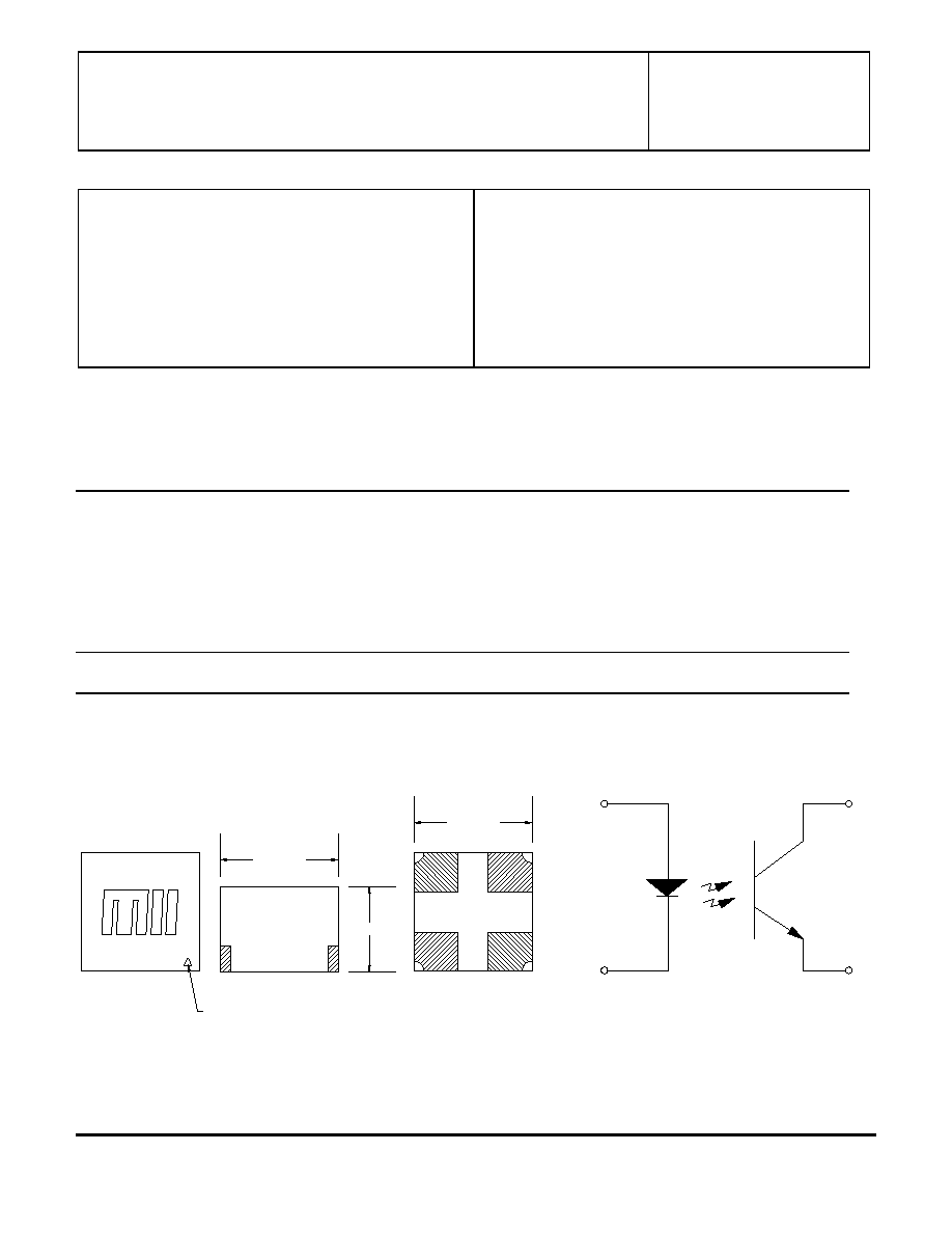
Package Dimensions Schematic Diagram
A
K
C
E
1
2
3
4
CATHODE
ANODE
COLLECTOR
EMITTER
BOTTOM VIEW
1
2
3
4
SIDE VIEW
TOP VIEW
PIN 1
0.090 [2.29]
0.090 [2.29]
ALL DIMENSIONS ARE IN INCHES [MILLIMETERS]
0.065 [1.65]
MICROPAC INDUSTRIES, INC.
OPTOELECTRONIC PRODUCTS DIVISION ∑ 725 E. Walnut St., Garland, TX 75040 ∑ (972) 272-3571 ∑ Fax (972) 487-6918
www.micropac.com
E-MAIL: optosales@micropac.com
5 - 11
66113
SINGLE CHANNEL, SURFACE MOUNT OPTOCOUPLER
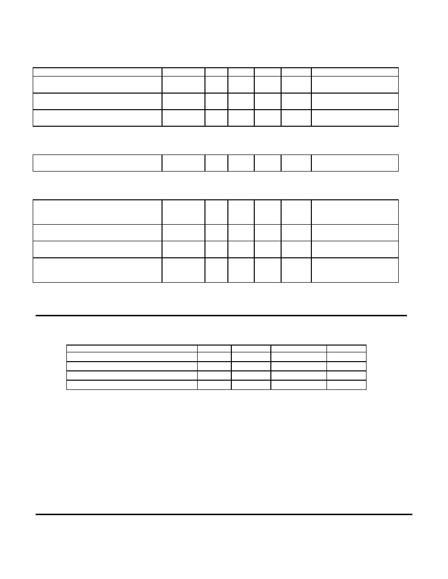
ELECTRICAL CHARACTERISTICS
T
A
= 25
∞C unless otherwise specified.
PARAMETER
SYMBOL
MIN
TYP
MAX
UNITS
TEST CONDITIONS
Input diode Static Reverse Current
I
R
100
µ
A
V
R
= 2V
Input Diode Static Reverse Voltage
V
R
2
V
I
R
= 10
µ
A
Input Diode Static Forward Voltage
V
F
1.6
V
I
F
= 20mA
OUTPUT TRANSISTOR
T
A
= 25
∞C unless otherwise specified.
Collector-Emitter Breakdown Voltage
V
(BR)CEO
35
V
I
C
= 1mA, I
B
= 0, I
F
= 0
COUPLED CHARACTERISTICS
T
A
= 25
∞C unless otherwise specified.
Current Transfer Ratio
-X01
T
a
= +25
∞
C
-X02
CTR
50
200
%
V
CE
= 5V, I
F
= 10mA
Off State Collector Current
I
C(OFF)
50
nA
V
CE
= 20V, I
F
= 0mA
Collector-Emitter Saturation Voltage
-X01
-X02
V
CE(SAT)
V
CE(SAT)
0.3
0.3
V
V
I
F
= 2mA, I
C
= 10mA, I
B
= 0
Rise Time
-X01
or
Fall Time
-X02
t
r
or
t
f
10
10
10
µ
s
V
CC
= 10V, I
F
= 5mA,
R
L
= 100
NOTES:
1.
The -001 and -002 are 100% tested at 25
∞
C only.
2.
The -101 and -102 are 100% are sample tested at temperature extremes.
3.
Custom electrical specifications are available.
RECOMMENDED OPERATING CONDITIONS:
PARAMETER
SYMBOL
MIN
MAX
UNITS
Input Current, Low Level
I
FL
0
100
µ
A
Input Current, High Level
I
FH
10
20
mA
Supply Voltage
V
CC
5.0
20
V
Operating Temperature
T
A
-55
125
∞
C