MICROPAC INDUSTRIES, INC.
OPTOELECTRONIC PRODUCTS DIVISION ∑ 725 E. Walnut St., Garland, TX 75040 ∑ (972) 272-3571 ∑ Fax (972) 487-6918
www.micropac.com
E-MAIL:
optosales@micropac.com
3 - 44
66163
SINGLE CHANNEL OPTOCOUPLERS
DIRECT REPLACEMENT FOR 3C91C
Mii
OPTOELECTRONIC PRODUCTS
DIVISION
REVISION C
12/29/00
Features:
∑ High
Reliability
∑ Base lead eliminated for improved noise immunity
∑ Rugged
package
∑ Stability over wide temperature
∑ +500V electrical isolation
Applications:
∑ Eliminate ground loops
∑ Level
shifting
∑ Line
receiver
∑ Switching power supplies
∑ Motor
control
DESCRIPTION
The 66163 contains a gallium arsenide infrared LED optically coupled to a silicon planar phototransistor. The optocoupler is
built on a TO-46 header. The collector of the phototransistor is electrically connected to the case. This optocoupler is
capable of transmitting signals between two galvanic sources. The potential difference between transmitter and receiver
should not go over the maximum isolation voltage. The internal base connection has been eliminated for improved noise
immunity.
ABSOLUTE MAXIMUM RATINGS
Input to Output Voltage...........................................................................................................................................................500V
Emitter-Collector Voltage............................................................................................................................................................5V
Collector-Emitter Voltage (Value applies to emitter-base open-circuited & the input-diode equal to zero) ............................60V
Reverse Input Voltage ...............................................................................................................................................................7V
Input Diode Continuous Forward Current at (or below) 65∞C Free-Air Temperature (see note 1) .....................................50mA
Peak Forward Input Current (Value applies for tw
<
1
µs
, PRR
<
300 pps) .......................................................................500mA
Continuous Collector Current ................................................................................................................................................50mA
Continuous Transistor Power Dissipation at (or below) 25∞C Free-Air Temperature (see Note 2) .................................230mW
Storage Temperature.......................................................................................................................................... -65∞C to +150∞C
Operating Free-Air Temperature Range ............................................................................................................. -55∞C to +125∞C
Lead Solder Temperature (10 seconds max.) .................................................................................................................... 260∞C
Notes:
1. Derate linearly to 125∞C free-air temperature at the rate of 0.67 mA/
∞
C above 65∞C.
2. Derate linearly to 125∞C free-air temperature at the rate of 2.3 mW/∞C.
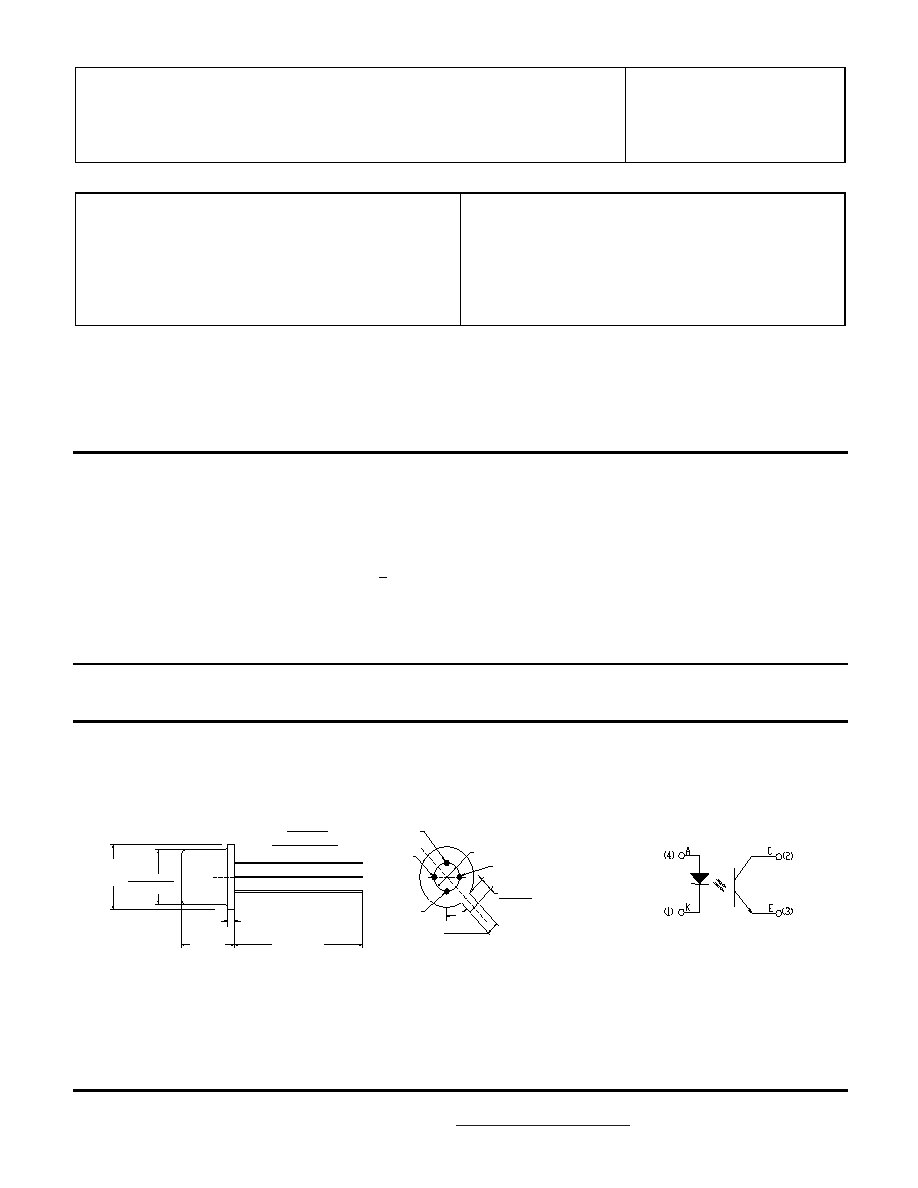
Package Dimensions Schematic Diagram
1
2
3
45∞
DIMENSIONS ARE IN INCHES (MILLIMETERS)
0.030 (0.76) MAX
0.178ÿ (4.52)
0.195ÿ (4.95)
0.230ÿ (5.84)
0.209ÿ (5.31)
4 LEADS
0.019ÿ (0.48)
0.016ÿ (0.41)
ÿ0.100[2.54]
0.50 [12.70] MIN
0.210 [5.34]
ANODE
0.048 [1.22]
0.046 [1.17]
EMITTER
COLLECTOR
CATHODE
4
0.170 [4.32]
0.028 [0.71]
0.036 [0.91]
NOTE: ANODE ELECTRICALLY CONNECTED TO CASE

MICROPAC INDUSTRIES, INC.
OPTOELECTRONIC PRODUCTS DIVISION ∑ 725 E. Walnut St., Garland, TX 75040 ∑ (972) 272-3571 ∑ Fax (972) 487-6918
www.micropac.com
E-MAIL:
optosales@micropac.com
3 - 45
66163
SINGLE CHANNEL OPTOCOUPLER
(Direct Replacement for 3C91C)
REVISION C 12/29/00
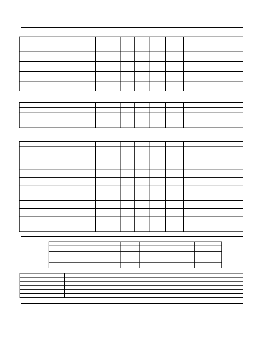
ELECTRICAL CHARACTERISTICS
T
A
= 25
∞C unless otherwise specified.
PARAMETER
SYMBOL
MIN
TYP
MAX
UNITS
TEST CONDITIONS
Input Diode Static Reverse Current
I
R
1
µA
V
R
= 3V
Input Diode Static Forward Voltage
V
F
1.15
1.2
V
I
F
= 2mA
Input Diode Static Forward Voltage
V
F
1.3
1.5
V
I
F
= 50mA
Reverse Breakdown Voltage
B
VR
7
12
V
I
R
= 100
µ
A
Input Diode Capacitance
C
IN
25
pF
V = 0V, f = 1MHz
OUTPUT TRANSISTOR
T
A
= 25
∞C unless otherwise specified.
PARAMETER
SYMBOL
MIN
TYP
MAX
UNITS
TEST CONDITIONS
Collector-Emitter Breakdown Voltage
V
(BR)CEO
50
V
I
C
= 1mA, I
B
= 0, I
F
= 0
Emitter-Collector Breakdown Voltage
V
(BR)ECO
7
V
I
C
= 0mA, I
E
= 10
µ
A, I
F
= 0
Collector-Emitter Dark Current
I
CEO1
I
CEO2
60
10
nA
nA
V
CE
= 50V, I
F
= 0mA
V
CE
= 5V, I
F
= 0mA
COUPLED CHARACTERISTICS
T
A
= 25
∞C unless otherwise specified.
PARAMETER
SYMBOL
MIN
TYP
MAX
UNITS
TEST CONDITIONS
On State Collector Current
I
C(ON)
4
mA
V
CE
= 5V, I
F
= 10mA
On State Collector Current
I
C(ON)
3
20
mA
V
CE
= 0.4V, I
F
= 10mA
On State Collector Current -55
∞
C
I
C(ON)
2
mA
V
CE
= 5V, I
F
= 10mA
On State Collector Current -X07
-107
I
C(ON)
20
mA
V
CE
= 5V, I
F
= 10mA
Collector-Emitter Saturation Voltage
V
CE(SAT)
0.4
V
I
F
= 50mA, I
C
= 10mA
Isolation Resistance
R
ISO
10
9
V
IN-OUT
= 500V
Input to Output Capacitance
C
IO
2
2.5
pF
f = 1MHz
Delay Time
t
d
2
4
µ
s
V
CE
= 5V, I
F
= 2mA, R
L
= 100
Storage Time
t
s
0.2
0.5
µ
s
V
CE
= 5V, I
F
= 2mA, R
L
= 100
Rise Time
t
r
3
5
µ
s
V
CE
= 5V, I
F
= 2mA, R
L
= 100
Fall Time
t
f
4
5
µ
s
V
CE
= 5V, I
F
= 2mA, R
L
= 100
RECOMMENDED OPERATING CONDITIONS:
PARAMETER
SYMBOL
MIN
MAX
UNITS
Input Current, Low Level
I
FL
0
1
µ
A
Input Current, High Level
I
FH
2
10
mA
Supply Voltage
V
CE
5
50
V
Operating Temperature
T
A
-55
125
∞
C
SELECTION GUIDE
PART NUMBER
PART DESCRIPTION
66163-001
Single Channel optocoupler, commercial (0
∞
to 70
∞
C)
66163-011
Single Channel optocoupler full military operating temperature range
66163-101
Single Channel optocoupler tested over full military temperature range with 100% device screening
66163-017
Single Channel optocoupler full military operating temperature range w/200% CTR
66163-107
Single Channel optocoupler tested over full military temperature range with 100% device screening w/200% CTR

