MICROPAC INDUSTRIES, INC.
OPTOELECTRONIC PRODUCTS DIVISION ∑ 725 E. Walnut St., Garland, TX 75040 ∑ (972) 272-3571 ∑ Fax (972) 487-6918
www.micropac.com
E-MAIL:
optosales@micropac.com
5 - 26
66169
GULL WING HERMETICALLY SEALED,
SINGLE CHANNEL OPTOCOUPLER
(Electrically Similar To 6N134)
Mii
OPTOELECTRONIC PRODUCTS
DIVISION
Rev 1 7/24/01
Features:
∑ High
Speed
∑ 1500 Vdc isolation test voltage
∑ 5 MHz bandwidth
∑ High radiation immunity
∑
Faraday shield to provide high
Common mode rejection
Applications:
∑ Military and Space
∑ High reliability systems
∑ Voltage Level Shifting
∑ Isolated Receiver Input
∑ Communication
systems
∑ Medical
systems
DESCRIPTION
The 66169 single channel optocoupler consists of an LED optically coupled to a high speed, high gain inverting detector
gate. Maximum isolation can be achieved while providing TTL output capable of switching with a propagation delay of 55ns
typical. The 66169 is a 10 pin gull wing hermetically sealed package and is available in standard and screened versions or
tested to customer specifications.
ABSOLUTE MAXIMUM RATINGS
Storage Temperature........................................................................................................................................... -65∞C to +150∞C
Operating Free-Air Temperature Range ............................................................................................................. -55∞C to +125∞C
Lead Solder Temperature.........................................................................................260∞C for 10s (1.6mm below seating plane)
Peak Forward Input Current ........................................................................................................................ 40mA (1ms duration)
Average Forward Input Current ............................................................................................................................................20mA
Input Power Dissipation .......................................................................................................................................................35mW
Reverse Input Voltage ...............................................................................................................................................................5V
Supply voltage-V
CC
................................................................................................................................... 7V(1 minute maximum)
Output Current-I
O
...................................................................................................................................................................25mA
Output Power Dissipation ....................................................................................................................................................40mW
Output Voltage ≠ V
O
..................................................................................................................................................................7V
Total Power Dissipation .....................................................................................................................................................350mW
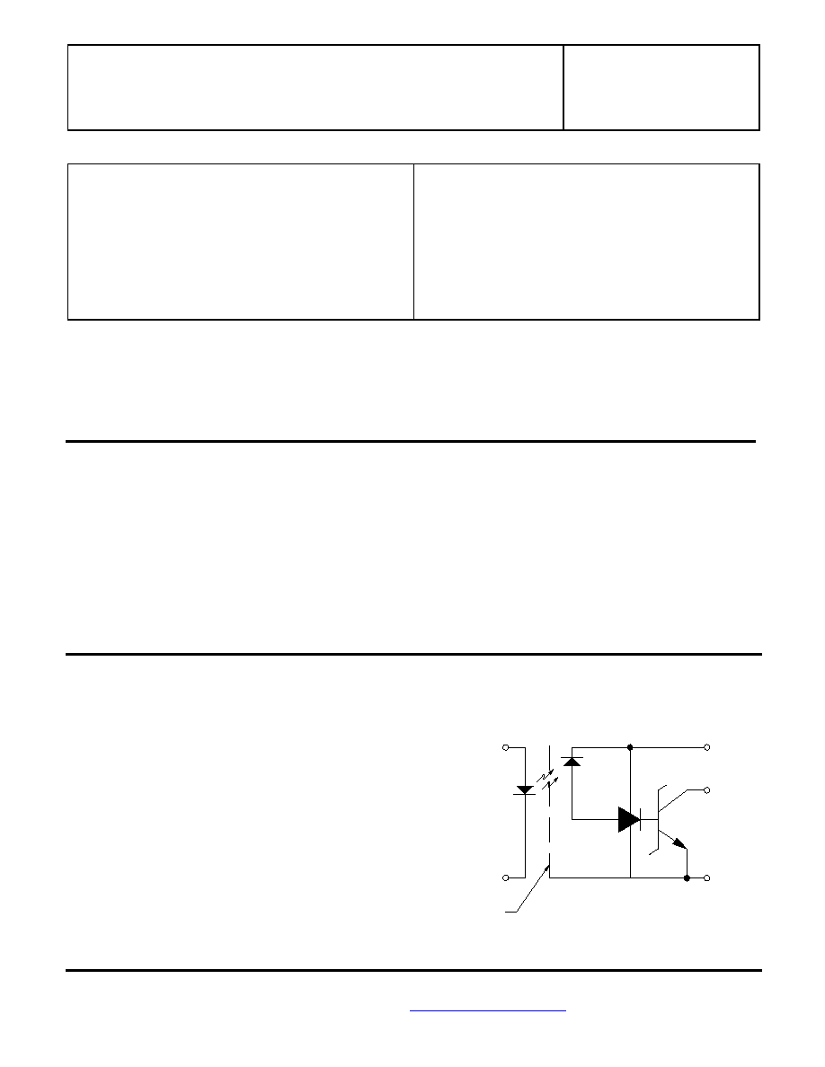
Package Dimensions Schematic Diagram
K
A
SHIELD
V OUT
GND
VCC
INFORMATION
AND PIN OUT
FOR PACKAGE
CONTACT FACTORY
MICROPAC INDUSTRIES, INC.
OPTOELECTRONIC PRODUCTS DIVISION ∑ 725 E. Walnut St., Garland, TX 75040 ∑ (972) 272-3571 ∑ Fax (972) 487-6918
www.micropac.com
E-MAIL:
optosales@micropac.com
5 - 27
66169
GULL-WING HERMETICALLY SEALED, DUAL CHANNEL OPTOCOUPLER
Rev 1 7/24/01
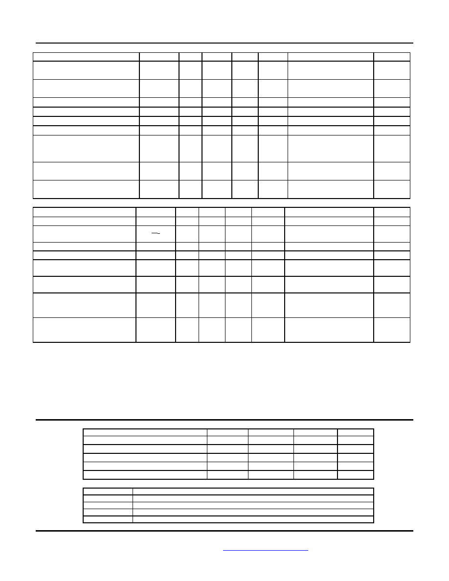
ELECTRICAL CHARACTERISTICS
T
A
= -55
∞
C to 125
∞
C unless otherwise specified.
PARAMETER
SYMBOL
MIN
TYP
MAX
UNITS
TEST CONDITIONS
NOTE
High Level Output Current
I
OH
5
250
µA
V
CC
= 5.5V, V
O
= 5.5V,
I
F
= 250µA
Low Level Output Voltage
V
OL
0.35
0.6
V
V
CC
= 5.5V, I
F
= 10mA
I
OL
(Sinking) = 10mA
8
High Level Supply Current
I
CCH
9
14
mA
V
CC
= 5.5V, I
F
= 0
Low Level Supply Current
I
CCL
13
18
mA
V
CC
= 5.5V, I
F
= 20mA
Input Forward Voltage
V
F
1.5
1.75
v
I
F
= 20mA
Input Reverse Breakdown Voltage
BV
R
5
v
I
R
= 10µA
Input-Output Insulation Leakage Current
I
I--O
1.0
µA
V
I--0
= 1500Vdc,
Relative Humidity = 45%
T
A
= 25∞C, t = 5s
3
Propagation Delay Time To High Output
Level
t
PLH
65
100
ns
V
CC
= 5.5V R
L
= 510
,
C
L
= 15Pf, I
f
= 13mA, T
A
= 25
∞
C
4
Propagation Delay Time To Low Output
Level
t
PHL
55
100
ns
V
CC
= 5.5V, R
L
= 510
,
C = 15p, I
f
= 13mA, T
A
= 25
∞
C
5
TYPICAL CHARACTERISTICS
AT T
A
= 25
∞
C, V
CC
= 5V Each Channel
PARAMETER
SYMBOL
MIN
TYP
MAX
UNITS
TEST CONDITIONS
NOTE
Input Capacitance
C
IN
60
pF
V
F
= 0, f = MHz
Input Diode Temperature Coefficient
v
F
T
A
-1.9
mV/
∞
C
I
F
= 20mA
Resistance (Input-Output)
R
I-0
10
12
V
I--O
= 500V
2
Capacitance (Input-Output)
C
I-0
1.7
pF
f = 1MHz
2
Input-Input Insulation Leakage Current
I
I-I
0.5
nA
Relative Humidity = 45%
V
I-I
= 500V, t = 5s
3
Output Rise-Fall Time (10-90%)
t
f
,
t
f
35
ns
R
L
= 510
, C
L
= 15pF
I
F
= 13mA
Common Mode Transient immunity at
High Output Level
CM
H
1000
10000
V/
µ
s
V
CM
= 10V (peak),
V
O
(min) = 2V,
R
L
= 510
, I
F
= 0mA
6
Common Mode Transient Immunity at
Low Output Level
CM
L
1000
10000
V/
µ
s
V
CM
= 10V (peak),
V
O
(max) = 0.8V,
R
L
= 510
, I
F
= 10mA
7
NOTES:
1.
Measured between pins 1 through 8 shorted together and pins 9 through 16 shorted together.
2.
Measured between pins 9 and 10 or 11 and 12 shorted together, and pins 9 through 16 shorted together.
3.
Measured between pins 9 and 10 shorted together, and pins 11 and 12 shorted together.
4. The
t
plh
propagation delay is measured from the 6.5mA point on the trailing edge of the input pulse to the 1.5V point on the trailing edge of the output
pulse.
5. The
t
phl
propagation delay is measured from the 6.5mA point on the leading edge of the input pulse to the 1.5V point on the leading edge of the output
pulse.
6. CM
h
is the max. tolerable common mode transient to assure that the output will remain in a high logic state (i.e. V
o
>
2.0V).
7. CM
l
is the max. tolerable common mode transient to assure that the output will remain in a low logic state (i.e. V
o
<
0.8V).
8.
It is essential that a bypass capacitor (.01 to 0.1
µ
F ceramic) be connected from pin 1 to pin 4.
RECOMMENDED OPERATING CONDITIONS:
PARAMETER
SYMBOL
MIN
MAX
UNITS
Input Current, Low Level
I
FL
0
250
µ
A
Input Current, High Level
I
FH
12.5
20
mA
Supply Voltage
V
C
4.5
5.5
V
Fan Out (TTL Load)
N
6
Operating Temperature
T
A
-55
125
∞
C
SELECTION GUIDE
PART NUMBER
PART DESCRIPTION
66169-000
Single Channel optocoupler, full mil-temp (-55
∞
to +125
∞
C) with 100% device screening
66169-002
Single Channel optocoupler, military operating range (-55
∞
to +125
∞
C)
66169-003
Single Channel optocoupler, commercial (0
∞
to 70
∞
C)
66169-004
Single Channel optocoupler, extended temperature range (-40
∞
to +85
∞
C)