
MICROPAC INDUSTRIES, INC.
OPTOELECTRONIC PRODUCTS DIVISION ∑ 725 E.Walnut Str., Garland, TX 75040 ∑ (972)272-3571 ∑ Fax (972)487-6918
www.micropac.com
E-MAIL: OPTOSALES @ MICROPAC.COM
5 - 40
66183
PROTON RADIATION TOLERANT OPTOCOUPLER
(Single Channel, Electrically Similar to 4N49)
Mii
OPTOELECTRONIC PRODUCTS
DIVISION
REVISION C 5/6/02
Features:
∑ High Reliability
∑ Base lead provided for conventional transistor
biasing
∑ Rugged package
∑ Stability over wide temperature
∑ +1000V electrical isolation
Applications:
∑ Eliminate ground loops
∑ Level shifting
∑ Line receiver
∑ Switching power supplies
∑ Motor control
DESCRIPTION
The 66183 is a single channel device electrically similar to the 4N49. This product has been designed to be more tolerant to
proton radiation. The 66183 optocoupler is packaged in a hermetically sealed 6 pin leadless chip carrier (LCC). This device
can be supplied to customer specifications as well as tested in accordance with MIL-PRF-19500 to Class S level.
ABSOLUTE MAXIMUM RATINGS
Input to Output Voltage........................................................................................................................................................... 1kV
Emitter-Base Voltage................................................................................................................................................................ 7V
Collector-Emitter Voltage (Value applies to emitter-base open-circuited & the input-diode equal to zero) ......................... 40V
Collector-Base Voltage ...........................................................................................................................................................45V
Reverse Input Voltage ............................................................................................................................................................. 2V
Input Diode Continuous Forward Current at (or below) 65∞C Free-Air Temperature (see note 1) ................................... 50mA
Peak Forward Input Current (Value applies for tw
1
µ
s, PRR
<
300 pps) ............................................................................. 1A
Continuous Collector Current ..............................................................................................................................................50mA
Continuous Transistor Power Dissipation at (or below) 25
∞
C Free-Air Temperature (see Note 2)................................ 300mW
Storage Temperature......................................................................................................................................... -55∞C to +150∞C
Operating Free-Air Temperature Range ............................................................................................................-55∞C to +100∞C
Lead Solder Temperature (10 seconds max.) .................................................................................................................. 240∞C
Notes:
1. Derate linearly to 100∞C free-air temperature at the rate of 0.80 mW/∞C above 25∞C.
2. Derate linearly to 100∞C free-air temperature at the rate of 3 mW/∞C above 25
∞C.
Package Dimensions Schematic Diagram
PIN 1
IDENTIFIER
2
1
6
5
4
3
ALL DIMENSIONS ARE IN INCHES [MILLIMETERS]
0.253 [6.42]
0.237 [6.01]
0.087 [2.22]
0.071 [1.81]
0.036 [0.91]
0.020 [0.51]
0.113 [2.87]
0.097 [2.46]
0.098 [2.49]
0.082 [2.08]
0.078 [1.99]
0.062 [1.58]
0.045 [1.14]
0.055 [1.40]
0.178 [4.52]
0.162 [4.11]
1
6
3
5
4
B
E
C
MICROPAC INDUSTRIES, INC.
OPTOELECTRONIC PRODUCTS DIVISION ∑ 725 E.Walnut Str., Garland, TX 75040 ∑ (972)272-3571 ∑ Fax (972)487-6918
www.micropac.com
E-MAIL: OPTOSALES @ MICROPAC.COM
5 - 41
66183
PROTON RADIATION TOLERANT OPTOCOUPLER
(Electrically similar to 4N49)
REVISION C 5/6/02
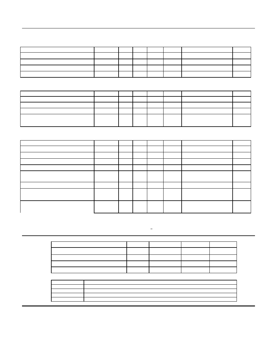
ELECTRICAL CHARACTERISTICS
T
A
= 25
∞
C unless otherwise specified.
PARAMETER SYMBOL
MIN
TYP
MAX
UNITS TEST
CONDITIONS NOTE
Input Diode Static Reverse Current
I
R
100 µA
V
R
= 3V
Input Diode Static Forward Voltage -55
∞
C V
F
1.0 2.2 V
I
F
= 10mA
Input Diode Static Forward Voltage +25
∞
C V
F
0.8 1.8 2.0
V
I
F
= 10mA
Input Diode Static Forward Voltage +100
∞
C V
F
0.8 2.2 V
I
F
= 10mA
OUTPUT TRANSISTOR
T
A
= 25
∞
C unless otherwise specified.
PARAMETER SYMBOL
MIN
TYP
MAX
UNITS TEST
CONDITIONS NOTE
Collector-Base Breakdown Voltage
V
(BR)CBO
45
V
I
C
= 100
µ
A, I
B
= 0, I
F
= 0
Collector-Emitter Breakdown Voltage
V
(BR)CEO
40
V I
C
= 1mA, I
B
= 0, I
F
= 0
Emitter-Base Breakdown Voltage
V
(BR)EBO
2
V
I
C
= 0mA, I
E
= 100
µ
A, I
F
= 0
Off-State Collector Current
+100
∞
C
I
CEO
I
CEO
100
100
nA
µ
A
V
CE
= 20V, I
F
= 0mA, I
B
= 0
V
CE
= 20V, I
F
= 0mA, I
B
= 0
COUPLED CHARACTERISTICS
T
A
= 25
∞
C unless otherwise specified.
PARAMETER SYMBOL
MIN
TYP
MAX
UNITS TEST
CONDITIONS NOTE
On State Collector Current
I
C(ON)
2.0 mA V
CE
= 5V, I
F
= 1mA, I
B
=0
On State Collector Current +100
∞
C I
C(ON)
2.0 mA V
CE
= 5.0V, I
F
= 2mA, I
B
=0
On State Collector Current -55
∞
C I
C(ON)
2.8 mA V
CE
= 5V, I
F
= 2mA, I
B
=0
Collector-Emitter Saturation Voltage
V
CE(SAT)
0.3 V
I
F
= 2mA, I
C
= 2mA
Input to Output Internal Resistance
R
IO
10
11
V
IN-OUT
= 1000V
1
Input to Output Capacitance
C
IO
2.5
5
pF
f = 1MHz, V
IN-OUT
= 1000V
1
Rise Time-Phototransistor Operation
t
r
10 25
µ
s V
CC
= 10V, I
F
= 10mA,
R
L
= 100
, I
B
= 0
Fall Time-Phototransistor Operation
t
f
10 25
µ
s V
CC
= 10V, I
F
= 10mA,
R
L
= 100
, I
B
= 0
NOTES:
1.
These parameters are measured between all phototransistor leads shorted together and with both input diode leads shorted together.
2.
This parameter must be measured using pulse techniques (t
W
= 100
µ
s duty cycle
<
1%).
RECOMMENDED OPERATING CONDITIONS:
PARAMETER SYMBOL
MIN
MAX
UNITS
Input Current, Low Level
I
FL
0 90
µ
A
Input Current, High Level
I
FH
2 10
mA
Supply Voltage
V
CE
5 10
V
Operating Temperature
T
A
-55 100
∞
C
SELECTION GUIDE
PART NUMBER
PART DESCRIPTION
66183-001
Single channel proton radiation tolerant optocoupler - commercial
66183-101
Single channel proton radiation tolerant optocoupler ≠ screened to JAN
66183-103
Single channel proton radiation tolerant optocoupler ≠ screened to JANTX
66183-105
Single channel proton radiation tolerant optocoupler ≠ screened to JANTXV