MICROPAC INDUSTRIES, INC.
OPTOELECTRONIC PRODUCTS DIVISION ∑ 725 E.Walnut Str., Garland, TX 75040 ∑ (972)272-3571 ∑ Fax (972)487-6918
www.micropac.com
E-MAIL: OPTOSALES @ MICROPAC.COM
5 - 38
66192
GULL WING HERMETICALLY SEALED,
SINGLE CHANNEL OPTOCOUPLER
(Electrical Equivalent To 66099)
Mii
OPTOELECTRONIC PRODUCTS
DIVISION
Rev A 6/6/02
Features:
∑ Current transfer ratio: 150% typical
∑ 1000 Vdc isolation test voltage
∑ Base lead provided for conventional transistor
biasing
∑ Low power consumption
∑
High radiation immunity
Applications:
∑ Military and Space
∑ High reliability systems
∑ Voltage Level Shifting
∑ Isolated Receiver Input
∑ Communication systems
DESCRIPTION
Radiation tests performed on the 66099 optocoupler have shown that the electrical performance of the device after irradiation
is an order of magnitude better than the 4N49 optocouplers. The 66192 has the same components and layout in a 10 pin,
hermetically sealed gull wing package. Figures 1 and 2 from the 66099 data sheet illustrate the radiation performance of the
device.
ABSOLUTE MAXIMUM RATINGS (t
a
=25∞C unless otherwise noted)
Storage Temperature........................................................................................................................................................-65∞C to +125∞C
Operating Free-Air Temperature Range ............................................................................................................-55∞C to +100∞C
Lead Solder Temperature (1/16in (1.6mm) from case for 10 seconds) ............................................................................ 240∞C
Input to Output Isolation Voltage.........................(see Note 1) ........................................................................................... 1kVdc
∑ Input Diode.
Peak Forward Input Current ...............................................................................................................................................40mA
Reverse Input Voltage ............................................................................................................................................................. 3V
Input Power Dissipation ...................................(see Note 2)..................................................................................... 80mW (2)
∑ Output Photodetector
Continuous Collector Current ..............................................................................................................................................50mA
Collector-Emitter Voltage......................................................................................................................................................150V
Emitter-Collector Voltage.......................................................................................................................................................... 4V
Collector-Base Voltage .........................................................................................................................................................150V
Power Dissipation................................................(see Note 3) ........................................................................................ 300mW
Notes:
1. Measured with input diode leads shorted together and output leads shorted together.
2. Derate linearly 0.80mW/∞C above 25∞C.
3. Derate linearly 1.07mW/∞C above 25∞C.
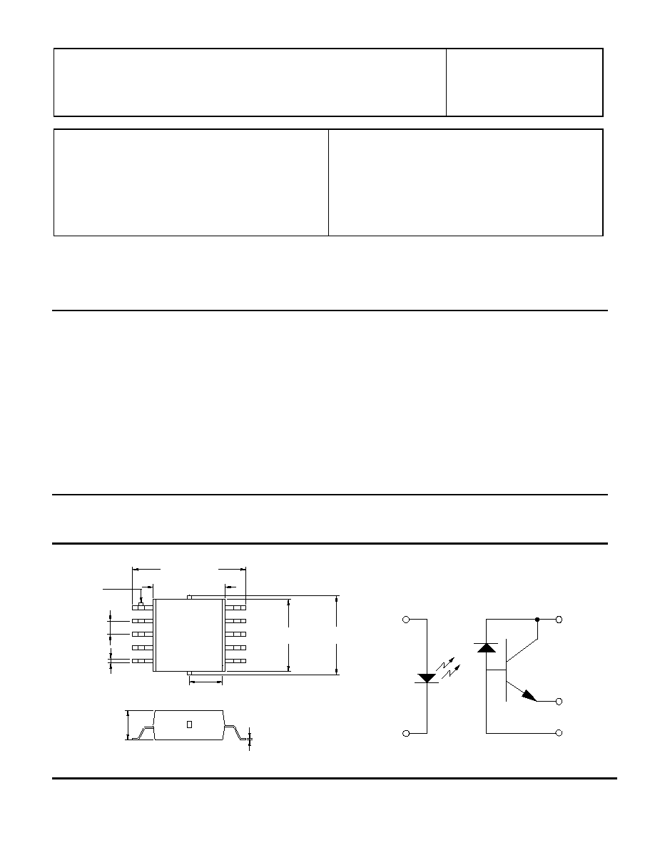
Package Dimensions Schematic Diagram
A
K
E
B
C
9
7
8
4
2
0.005 [0.127]
0.110 [2.784]
ALL DIMENSIONS ARE IN INCHES [MILLIMETERS]
0.425 [10.795]
0.270 [6.858]
PIN 1
0.050 [1.270]
0.015 [0.381]
±.003 [0.076]
0.295 [7.493]
0.270 [6.858]
0.125 [3.175]
MICROPAC INDUSTRIES, INC.
OPTOELECTRONIC PRODUCTS DIVISION ∑ 725 E.Walnut Str., Garland, TX 75040 ∑ (972)272-3571 ∑ Fax (972)487-6918
www.micropac.com
E-MAIL: OPTOSALES @ MICROPAC.COM
5 - 39
66192
GULL-WING PACKAGE, SINGLE CHANNEL, RADIATION TOLERANT OPTOCOUPLER
Rev A
6/6/02
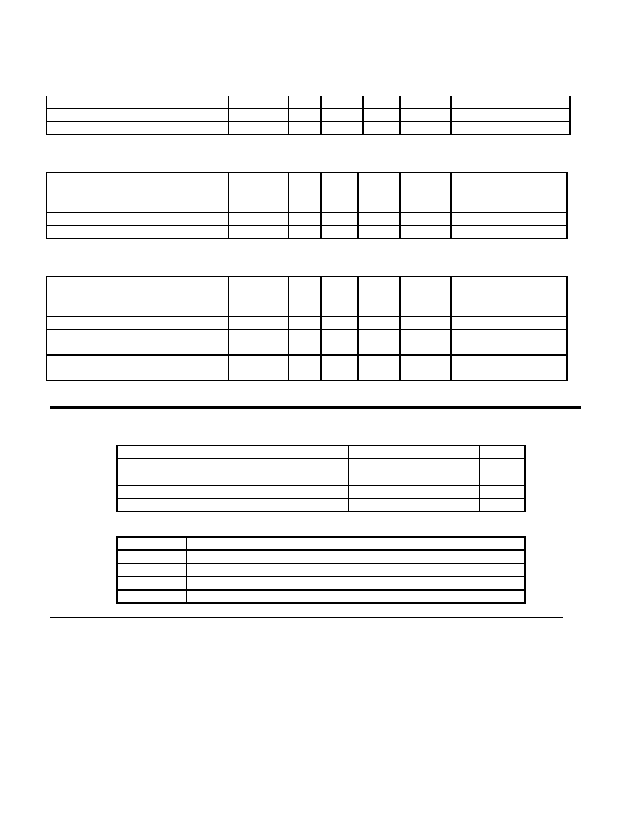
ELECTRICAL CHARACTERISTICS
T
A
= 25
∞
C unless otherwise specified.
PARAMETER SYMBOL
MIN
TYP
MAX UNITS TEST
CONDITIONS
Input Diode Static Reverse Current
I
R
100 µA
V
R
= 2V
Input Diode Static Forward Voltage
V
F
0.8 2 V
I
F
= 10mA
OUTPUT TRANSISTOR CHARACTERISTICS
T
A
= 25
∞
C unless otherwise noted
PARAMETER SYMBOL
MIN
TYP
MAX UNITS TEST
CONDITIONS
Collector-Base Breakdown Voltage
V
(BR)CBO
150
V
I
C
= 100
µ
A, I
F
= 0
Collector-Emitter Breakdown Voltage
V
(
BR)CEO
150
V
I
C
= 1mA, I
B
= 0, I
F
= 0
Emitter-Base Breakdown Voltage
V
(BR)EBO
4
V I
E
= 100
µ
A, I
F
= 0
Collector-Emitter Cutoff Current
I
CEO
100 nA
V
CE
= 20V
COUPLED CHARACTERISTICS
T
A
= 25
∞
C unless otherwise noted
PARAMETER SYMBOL
MIN
TYP
MAX UNITS TEST
CONDITIONS
Current Transfer Ratio
CTR
100
%
V
CE
= 1V, I
F
= 10mA
Collector-Emitter Saturation Voltage
V
CE(SAT)
0.3 V
I
F
= 20mA, I
C
= 10mA
Input-Output Isolation Current
I
ISO
100 nA
V
I-O
= 1000V
Rise Time
t
r
20
µ
s V
CC
= 10V, I
F
= 10mA,
R
L
= 100
Fall Time
t
f
20
µ
s V
CC
= 10V, I
F
= 10mA,
R
L
= 100
RECOMMENDED OPERATING CONDITIONS:
PARAMETERS SYMBOL
MIN
MAX
UNITS
Input Current, Low Level
I
FL
0 100
µ
A
Input Current, High Level
I
FH
10 20
mA
Supply Voltage
V
CC
5.0 100
V
Operating Temperature
T
A
-55 +100
∞
C
SELECTION GUIDE
PART NUMBER
PART DESCRIPTION
66192-000
Single Channel optocoupler, full mil-temp (-55
∞
to +100
∞
C) with 100% device screening
66192-002
Single Channel optocoupler, military operating range (-55
∞
to +100
∞
C)
66192-003
Single Channel optocoupler, commercial (0
∞
to 70
∞
C)
66192-004
Single Channel optocoupler, extended temperature range (-40
∞
to +85
∞
C)