MICROPAC INDUSTRIES, INC.
OPTOELECTRONIC PRODUCTS DIVISION ∑ 725 E.Walnut St., Garland, TX 75040 ∑ (972) 272-3571 ∑ Fax (972) 487-6918
www.micropac.com
E-MAIL:
optosales@micropac.com
66229
CONSTANT CURRENT TRANSFER RATIO,
SINGLE CHANNEL
OPTOCOUPLERS, SCREENED TO JAN, JANTX, JANTXV
Mii
OPTOELECTRONIC PRODUCTS
DIVISION
10/17/02 Rev B
Features:
∑ Vin (volts) =Iout (mA)
∑ Vin/Iout is constant within 4.0% over temperature
∑ Minimum component count for high reliability
∑ Rugged package (TO-5 )
∑ Internal amplifier for regulation
∑ Rugged output transistor
Applications:
∑ Eliminate ground loops
∑ Level shifting of signals
∑ Line receiver
∑ Power supply feedback loops
∑ Motor control
∑ Signal Isolation
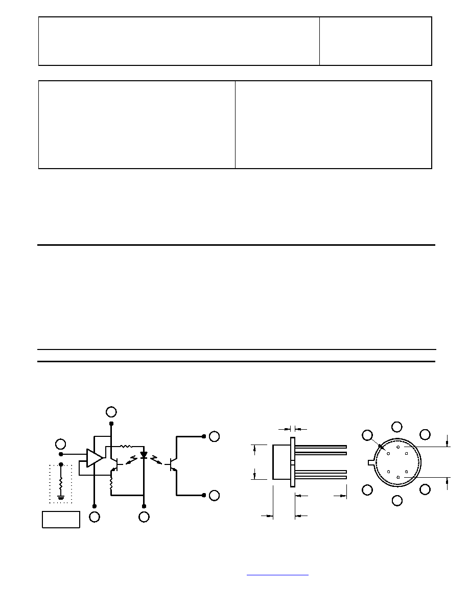
DESCRIPTION
A Gallium Aluminum Arsenide (GaAlAs) infrared LED controlled by a high gain op amp illuminates two matched
phototransistors, one of which provides feedback to the op amp allowing a consistent output from the other. The regulation
provides protection against output signal degradation normally associated with time, temperature and even radiation. The
66229 can be tested to customer specifications, as well as to MIL-PRF-19500 JAN, JANTX, JANTXV and JANS quality levels.
CTR degradation worries are gone when you use the 66229.
ABSOLUTE MAXIMUM RATINGS
Input to Output Voltage.........................................................................................................................................................1000V
Emitter-Collector Voltage............................................................................................................................................................7V
Collector-Emitter Voltage .........................................................................................................................................................40V
Reverse Input Voltage ............................................................................................................................................................0.1V
Continuous Output Phototransistor Collector Current...........................................................................................................10mA
Power Supply Voltage ......................................................................................................................................................+15Volts
Negative Supply Voltage........................................................................................................................-15Volts
Storage Temperature........................................................................................................................................... -65∞C to +125∞C
Operating Free-Air Temperature Range ............................................................................................................. -55∞C to +125∞C
Lead Solder Temperature (1/16" (1.6mm) from case for 10 seconds) ................................................................................ 240∞C
Notes:
External
Resistor
1
3
7
2
6
5
R
R
Vcc (+)
Vee (-)
Collector
Emitter
Vin
GND
0.325
0.040
MAX
0.500
MIN
0.170
0.220
BOTTOM VIEW
Schematic Diagram
g
+
_
1
2
3
5
6
7

MICROPAC INDUSTRIES, INC.
OPTOELECTRONIC PRODUCTS DIVISION ∑ 725 E.Walnut St., Garland, TX 75040 ∑ (972) 272-3571 ∑ Fax (972) 487-6918
www.micropac.com
E-MAIL:
optosales@micropac.com
66229
CONSTANT CURRENT TRANSFER RATIO, SINGLE OPTOCOUPLERS
SCREENED TO JAN, JANTX, JANTXV
10/17/02 Rev B
ELECTRICAL CHARACTERISTICS
T
A
= 25
∞
C Unless otherwise specified
PARAMETER SYMBOL
MIN
TYP
MAX
UNITS TEST
CONDITIONS
Input Signal
V
in
0
10
volts
Vcc = +15 volts, V
EE
= -5V
OUTPUT TRANSISTOR
T
A
= 25
∞
C Unless otherwise specified
PARAMETER SYMBOL
MIN
TYP
MAX
UNITS TEST
CONDITIONS
Collector-Base Breakdown Voltage
V
(BR)CBO
40
V
Iin = 0, Vcc=0
Collector-Emitter Breakdown Voltage
V
(BR)CEO
40
V
Iin =0, Vcc=0
Emitter-Collector Breakdown Voltage
V
(BR)EBO
7
V
Iin = 0, Vcc=0
COUPLED CHARACTERISTICS
T
A
= 25
∞
C Unless otherwise specified
PARAMETER SYMBOL
MIN
TYP
MAX
UNITS TEST
CONDITIONS
Supply Voltage
Vcc
7 12 15 VDC
Supply Voltage
V
EE
-3 -5 -15 VDC
On State Collector Current
I
C(ON)
0.5
5
mA
Vcc = +15volts, Vin = .5< 5volts
Off State Collector Current
I
C(OFF)
0 100
µ
A
Vcc = 15volts, Vin = 0volts
Collector ≠ Emitter Saturation Voltage
Vce(sat)
0.3
0.5
Volts
Vcc = 15 volts, Vin = 5volts
Rise time/ Fall time
tr/tf
5.0
µ
S
Vcc = 15 volts, Vin = 5volts
Input to Output Resistance
R
I-O
10
11
V
IN-OUT
= 1kV
Input to Output Capacitance
C
I-O
5
pF
f = 1MHz, V
IN-OUT
= 1kV
Delay Time T
DR
& T
DF
t
D
5.0
µ
S
V
CC
= 12V
RECOMMENDED OPERATING CONDITIONS:
PARAMETER SYMBOL
MIN
MAX
UNITS
Input Current, Low Level
I
FL
0 100
µA
Input Current, High Level
I
FH
2 10 mA
Supply Voltage
Supply Voltage
V
CC
V
EE
+5
-15
+15
-3
VDC
VDC
MICROPAC INDUSTRIES, INC.
OPTOELECTRONIC PRODUCTS DIVISION ∑ 725 E.Walnut St., Garland, TX 75040 ∑ (972) 272-3571 ∑ Fax (972) 487-6918
www.micropac.com
E-MAIL:
optosales@micropac.com
66229
CONSTANT CURRENT TRANSFER RATIO, SINGLE OPTOCOUPLERS
SCREENED TO JAN, JANTX, JANTXV
10/17/02 Rev B
t ,
0
2
1
3
7
4
5
6
3
0
1
2
4
5
6
7
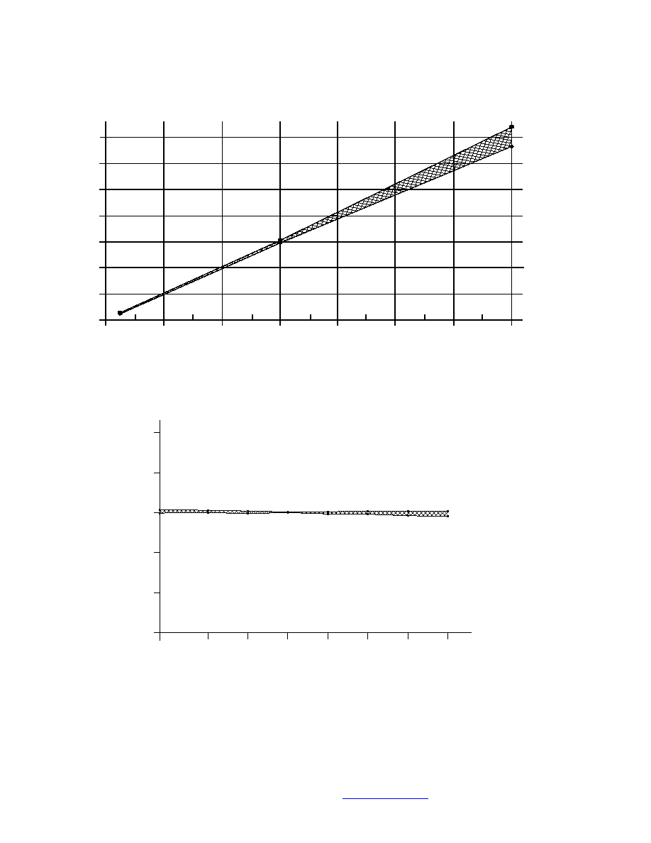
V in , V o lt s
± 1 0 %
± 2 %
± 5 %
I n p u t - O u t p u t L in e a r it y
O v e r 0 . 2 5 0 V t o 7 . 0 0 V I n p u t
Iout,
mA
5
100
-55
-25
75
50
25
0
TEMPERATURE, ∞C
1
2
3
4
125
0
VARIATION OVER TEMPERATURE
(Vin = 3.0 V)