1500 WATT LOW VOLTAGE TRANSIENT
VOLTAGE SUPPRESSOR
S C O T T S D A L E D I V I S I O N
1N5907 and 1N5908
W
W
W
.
Mi
c
r
o
s
e
m
i
.
C
O
M
1
N
5
9
0
7
t
h
r
u
1
N
5
9
0
8
DESCRIPTION
APPEARANCE
This pair of unidirectional low voltage Transient Voltage Suppressor (TVS)
devices for the 1N5907 and 1N5908 JEDEC registrations with different
packages have the same high Peak Pulse Power rating of 1500 W with
extremely fast response times. The 1N5907 is available in a military qualified
version as described in the Features section herein. They are most often used
for protecting against transients from inductive switching environments, induced
RF effects, or induced secondary lightning effects as found in surge levels of
IEC61000-4-5 described herein. They are also very successful in protecting
airborne avionics and electrical systems when low voltage is required. Since
their response time is virtually instantaneous, they can also protect from ESD
and EFT per IEC61000-4-2 and IEC61000-4-4.
Both hermetic seal and molded types are available.
CASE 1
DO-13
(DO-202AA)
IMPORTANT: For the most current data, consult MICROSEMI's website:
http://www.microsemi.com
FEATURES
APPLICATIONS / BENEFITS
� Unidirectional TVS series for thru-hole mounting
� Suppresses transients up to 1500 watts @ 10/1000 �s (Figure 1)
in less than 100 pico seconds
� Low working voltage (V
WM
) of 5 V
� Hermetic sealed DO-13 metal package for 1N5907 and plastic
"Case 1" for 1N5908
� JAN/TX/TXV military qualification available for 1N5907 per MIL-
PRF-19500/500 by adding JAN, JANTX, or JANTXV prefix, e.g.
JANTXV1N5907
� Surface mount equivalent packages also available as SMCJ5.0
or SMCG5.0 in separate data sheet (consult factory for other
surface mount options)
� Protection from switching transients and induced RF
� Protects TTL, ECL, DTL, MOS, MSI, and other
integrated circuits requiring 5.0 V or lower power
supplies
� Protection from ESD and EFT per IEC 61000-4-2 and
IEC 61000-4-4
� Secondary lightning protection per IEC61000-4-5 with
42 Ohms source impedance: Class 1 thru 4
� Secondary lightning protection per IEC61000-4-5 with
12 Ohms source impedance: Class 1 thru 4
� Secondary lightning protection per IEC61000-4-5 with
2 Ohms source impedance: Class 2 & 3
�
1N5907 Inherently radiation hard as described in
Microsemi MicroNote 050
MAXIMUM RATINGS
MECHANICAL AND PACKAGING
� 1500 Watts for 10/1000 �s at lead temperature (T
L
) 25
o
C (See Figs.
1, 2, and 4) with repetition rate of 0.01% or less*
� Operating & Storage Temperatures: -65
o
to +175
o
C for 1N5907
and
-65
o
to +150
o
C for 1N5908
� THERMAL RESISTANCE (junction to lead): 50
o
C/W for 1N5907 or
22
o
C/W for 1N5908 at 0.375 inches (10 mm) from body
� THERMAL RESISTANCE (junction to ambient): 110
o
C/W for
1N5907, or 82
o
C/W for 1N5908 when mounted on FR4 PC board
with 4 mm
2
copper pads (1 oz) and track width 1 mm, length 25 mm
� DC Power Dissipation* (1N5907): 1 Watt at T
L
<125
o
C 3/8" (10
mm) from body, or 1 Watt at T
A
+65
o
C when mounted on FR4 PC
board as described for thermal resistance junction to ambient
� DC Power Dissipation* (1N5908): 5 Watts at T
L
<+40
o
C 3/8" (10
mm) from body, or 1.52 Watts at T
A
= +25
o
C when mounted on FR4
PC board as described for thermal resistance junction to ambient
� Forward surge current: 200 A for 8.3ms half-sine wave at T
A
=
+25
o
C
� Solder Temperatures: 260
o
C for 10 s (maximum)
� CASE (1N5907): DO-13 (DO-202AA) welded
hermetically sealed metal and glass
� Case (1N5908): "Case 1" Void Free transfer molded
thermosetting epoxy body meeting UL94V-0
� FINISH: External metal surfaces are Tin-Lead (Sn-
Pb) plated and solderable per MIL-STD-750 method
2026
� POLARITY: Polarity indicated by diode symbol or
cathode band (cathode connected to case for 1N5907)
� MARKING: Part number and polarity symbol
� WEIGHT: 1.4 grams. (Approx)
� TAPE & REEL option: Standard per EIA-296 (add
"TR" suffix to part number)
� See package dimension on last page
*
TVS devices are not typically used for dc power dissipation and are instead operated at or less than their rated standoff voltage
(V
WM
) except for transients that briefly drive the device into avalanche breakdown (V
BR
to V
C
region).
Microsemi
Scottsdale Division
8700 E. Thomas Rd. PO Box 1390, Scottsdale, AZ 85252 USA, (480) 941-6300, Fax: (480) 947-1503
Page 1
Copyright
2002
11-06-2003 REV A

1500 WATT LOW VOLTAGE TRANSIENT
VOLTAGE SUPPRESSOR
S C O T T S D A L E D I V I S I O N
1N5907 and 1N5908
W
W
W
.
Mi
c
r
o
s
e
m
i
.
C
O
M
1
N
5
9
0
7
t
h
r
u
1
N
5
9
0
8
ELECTRICAL CHARACTERISTICS @ 25
o
C
JEDEC
Type
No.
Reverse
Standoff
Voltage
V
WM
(NOTE 1)
Volts
Minimum
Breakdown
Voltage
V
(BR)
@ 1 mA
Volts
Maximum
Standby
Current
I
D
@ V
WM
�A
Maximum
Clamping
Voltage
V
C
@ I
PP1
(FIG. 3)
Volts
Peak Pulse
Current
I
PP1
(FIG. 3)
Amps
Maximum
Clamping
Voltage
V
C
@ I
PP2
(FIG. 3)
Volts
Peak Pulse
Current
I
PP2
(FIG. 3)
Amps
Maximum
Clamping
Voltage
V
C
@ I
PP3
(FIG. 3)
Volts
Peak Pulse
Current
I
PP3
(FIG. 3)
Amps
1N5907*
1N5908
5.0
5.0
6.0
6.0
300
300
7.6
7.6
30
30
8.0
8.0
60
60
8.5
8.5
120
120
* Also available in military qualified types with a JAN, JANTX, or JANTXV prefix per MIL-PRF-19500/500.
NOTE 1: A TVS is normally selected according to the reverse "Standoff Voltage" V
WM
which should be equal to or greater than the dc or
continuous peak operating voltge level.
SYMBOLS & DEFINITIONS
Symbol Definition
V
WM
Standoff Voltage: Applied Reverse Voltage to assure a nonconductive condition. (See Note 1 above)
V
(BR)
Breakdown Voltage: This is the Breakdown Voltage the device will exhibit at 25
o
C
V
C
Maximum Clamping Voltage: The maximum peak voltage appearing across the TVS when subjected to the
peak pulse current in a one millisecond time interval. The peak pulse voltage is the combination of voltage rise
due to both the series resistance and thermal rise and positive temperature coefficient (
V(BR)
)
I
PP
Peak Pulse Current: The peak current during the impulse (See Figure 2)
P
PP
Peak Pulse Power: The pulse power as determined by the product of V
C
and I
PP
I
D
Standby Current: The current at the standoff voltage (V
WM
)
I
(BR)
Breakdown Current: The current used for measuring Breakdown Voltage (V
(BR)
)
GRAPHS
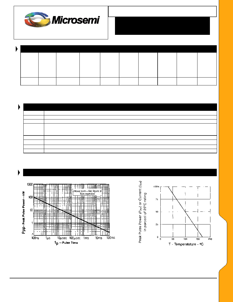
FIGURE 1
FIGURE 2
PEAK PULSE POWER VS. PULSE TIME
DERATING CURVE
Microsemi
Scottsdale Division
8700 E. Thomas Rd. PO Box 1390, Scottsdale, AZ 85252 USA, (480) 941-6300, Fax: (480) 947-1503
Page 2
Copyright
2002
11-06-2003 REV A


