1
2N2907ADIE
A Microsemi Company
580 Pleasant St.
Phone: 617-924-9280
Watertown, MA 02172
Fax: 617-924-1235
DIE SPECIFICATION
SWITCHING TRANSISTOR
PNP SILICON
FEATURES:
n
ELECTRICAL PERFORMANCE I.A.W. MIL-PRF-19500/291
n
AVAILABLE IN WAFER OR CHIP FORM FOR HYBRID APPLICATIONS
n
GENERAL PURPOSE-HIGH SPEED SWITCHING APPLICATIONS
n
LOW VCE(sat): .4V @ IC = 150 mAdc
Absolute Maximum Ratings:
Symbol
Parameter
Limit
Unit
Vceo
Collector-Emitter Voltage
60
Vdc
Vcbo
Collector-Base Voltage
60
Vdc
Vebo
Emitter-Base Voltage
5.0
Vdc
Ic
Collector Current- Continuous
600
mAdc
Tj, Tstg
Operating Junction & Storage
-65 to +200 �C
Temperature Range
Sertech reserves the right to make changes to any product design, specification, or other information at any time without
prior notice.
Data Sheet, Die, 2N2907A MSW Rev. - 4/14/98
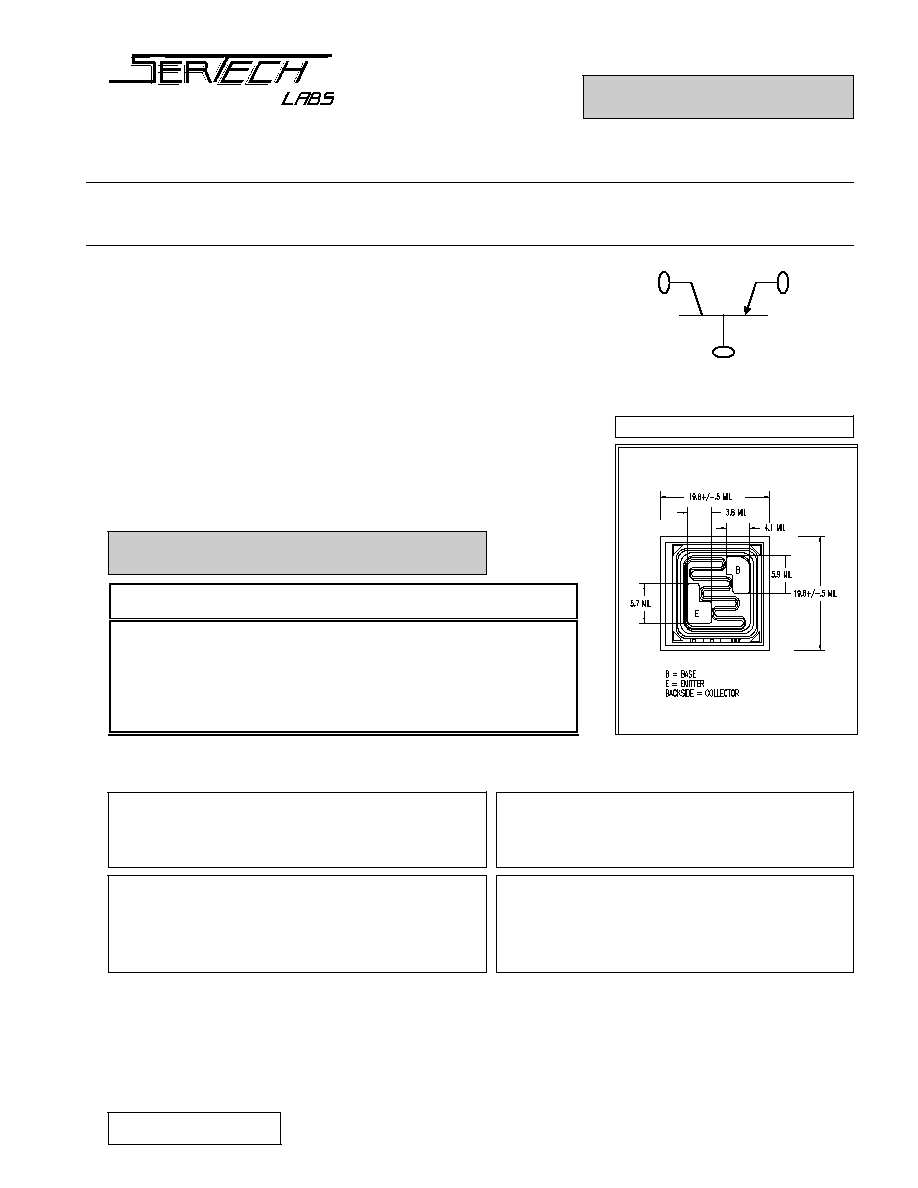
PHYSICAL DIMENSIONS
Packaging Options:
W: Wafer (100% probed) U: Wafer (sample probed)
D: Chip (Waffle Pack) B: Chip (Vial)
V: Chip (Waffle Pack, 100% visually inspected) X: Other
Processing Options:
Standard: Capable of JANTXV applications (No Suffix)
Suffix C: Commercial
Suffix S: Capable of S-Level equivalent applications
Metallization Options:
Standard: Al Top / Au Backside (No Dash #)
Dash 1: Al Top / TiPdAg Backside
ORDERING INFORMATION:
PART #: 2N2907A_ _ - _
First Suffix Letter: Packaging Option
Second Suffix Letter: Processing Option
Dash #: Metallization Option
MSC0948.PDF

2
Electrical Characteristics @ Tj = 25
�
C
Symbol
Parameter
Conditions
Min Max Unit
OFF CHARACTERISTICS
V(BR)CBO
Breakdown Voltage, Collector to Base
Bias Cond. D, IC=10uAdc
60
Vdc
V(BR)EBO
Breakdown Voltage, Emitter to Base
Bias Cond. D, IE=10uAdc
5
Vdc
V(BR)CEO
Breakdown Voltage, Collector to Emitter
Bias Cond. D, IC= 10mAdc, pulsed
60
Vdc
ICES
Collector to Emitter Cutoff Current
Bias Cond. D, VCE=50Vdc
50 nAdc
ICBO1
Collector to Base Cutoff Current
Bias Cond. D, VCB=50Vdc
10 nAdc
IEBO
Emitter to Base Cutoff Current
Bias Cond. D, VEB= 4Vdc
50 nAdc
ON CHARACTERISTICS
hFE1
Forward-Current Transfer Ratio
VCE=10Vdc, IC=0.1mAdc
75
hFE2
Forward-Current Transfer Ratio
VCE=10Vdc, IC=1.0mAdc
100 450
hFE3
Forward-Current Transfer Ratio
VCE=10Vdc, IC=10mAdc
100
hFE4
Forward-Current Transfer Ratio
VCE=10Vdc, IC=150mAdc, pulsed
100 300
hFE5
Forward-Current Transfer Ratio
VCE=10Vdc, IC=500mAdc, pulsed
50
VCE(sat)1
Collector to Emitter Saturation Voltage
IC=150mAdc, IB=15mAdc, pulsed
0.4 Vdc
VCE(sat)2
Collector to Emitter Saturation Voltage
IC=500mAdc, IB=50mAdc, pulsed
1.6 Vdc
VBE(sat)1
Base to Emitter Saturation Voltage
IC=150mAdc, IB=15mAdc, pulsed
0.6
1.3 Vdc
VBE(sat)2
Base to Emitter Saturation Voltage
IC=500mAdc, IB=50mAdc, pulsed
2.6 Vdc
SMALL SIGNAL CHARACTERISTICS
hfe
Short Circuit Forward Current Xfer Ratio
VCE= 10Vdc,IC =1mAdc, f= 1kHz
100
/hfe/
Magnitude of Short Circuit Forward
VCE= 20Vdc,IC =50mAdc, f=100MHz
2
Current Transfer Ratio
Cobo
Output Capacitance
VCB= 10Vdc, IE =0, 100kHz< f <1MHz
8 pF
Cibo
Input Capacitance
VEB= 2.0Vdc, IC=0, 100kHz< f <1MHz
30 pF
SWITCHING CHARACTERISTICS
ton
Saturated Turn-on Time
As defined in 19500/291 Figure 7
45 nS
toff
Saturated Turn-off Time
As defined in 19500/291 Figure 8
300 nS