
2N3251A
60 Volts
200 mAmps
Features
∑
Meets MIL-S-19500/323
∑
Collector-Base Voltage 60V
∑
Collector Current: 200 mA
∑
Fast Switching 370 nS
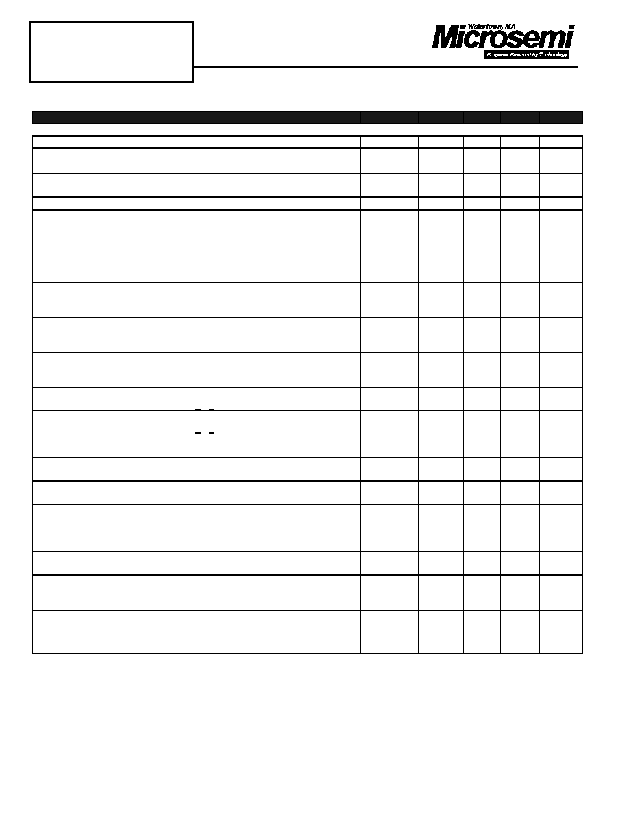
RATING
SYMBOL
MAX.
UNIT
Collector-Emitter Voltage
V
CEO
-60
Vdc
Collector-Base Voltage
V
CBO
-60
Vdc
Emitter-Base Voltage
V
EBO
-5.0
Vdc
Collector Current
I
C
-200
mAdc
Total Device Dissipation
@ T
A
= 25
o
C
Derate above 25
o
C
P
D
0.36
2.4
Watts
mW/
o
C
Total Device Dissipation
@ T
C
= 25
o
C
Derate above 25
o
C
P
D
1.2
8
Watts
mW/
o
C
Operating Temperature Range
T
J
-65 to
+175
o
C
Storage Temperature Range
T
S
-65 to
+175
o
C
Thermal Resistance, Junction to Ambient
R
JA
417
o
C/W
Thermal Resistance, Junction to Case
R
JC
146
o
C/W
Maximum Ratings
Datasheet# MSC0281A 5/19/97
PNP
BIPOLAR
TRANSISTOR
580 Pleasant St.
Watertown, MA 02172
PH: (617) 926-0404
FAX: (617) 924-1235
Mechanical Outline
CHARACTERISTICS
SYMBOL
MIN.
TYP.
MAX.
UNIT
Off Characteristics
Collector-Emitter Breakdown Voltage(1) (I
C
= -10 mAdc)
BV
CEO
-60
--
Vdc
Collector-Base Breakdown Voltage (I
C
= -10
µ
Adc)
BV
CBO
-60
--
Vdc
Emitter-Base Breakdown Voltage (I
E
= -10
µ
Adc)
BV
EBO
-5.0
--
Vdc
Collector Cutoff Current (V
CE
= -40 Vdc, V
EB
= -3.0 Vdc)
( at 150 C )
I
CEX
--
-20
-20
nA
uA
Base Cutoff Current (V
CE
= -40 Vdc, V
EB
= -3.0 Vdc)
I
BEX
--
-50
nAdc
D.C. Current Gain
(I
C
= -0.1 mAdc, V
CE
= -1.0 Vdc)
(I
C
= -1.0 mAdc, V
CE
= -1.0 Vdc)
(I
c
= -1.0mAdc, V
CE
= -1.0Vdc) @ -55C
(I
C
= -10 mAdc, V
CE
= -1.0 Vdc)(1)
(I
C
= -50 mAdc, V
CE
= -1.0 Vdc)(1)
h
FE
80
90
40
100
30
--
--
--
300
--
--
Collector-Emitter Saturation Voltage(1)
(I
C
= -10 mAdc, I
B
= -1.0 mAdc)
(I
C
= -50 mAdc, I
B
= -5.0 mAdc)
V
CE(Sat)
--
--
-0.25
-0.5
Vdc
Base-Emitter Saturation Voltage(1)
(I
C
= -10 mAdc, I
B
= -1.0 mAdc)
(I
C
= -50 mAdc, I
B
= -5.0 mAdc)
V
BE(Sat)
-0.6
--
-0.9
-1.2
Vdc
Magnitude of common emitter small-signal short-circuit forward current
transfer ratio
(I
C
= -10 mAdc, V
CE
= -20 Vdc, f = 100MHz)
/h
fe
/
3.0
9.0
Output Capacitance
(V
CB
= -10 Vdc, I
E
= 0, 100kHz < f < 1MHz)
C
OBO
--
6.0
pf
Input Capacitance
(V
EB
= -10 Vdc, I
C
= 0, 100kHz < f < 1MHz)
C
IBO
--
8.0
pf
Input Impedance
(I
C
= -1.0 mA, V
CE
= -10 V, f = 1.0 kHz)
h
je
2.0
12
kohms
Voltage Feedback Ratio
(I
C
= -1.0 mA, V
CE
= -10 V, f = 1.0 kHz)
h
re
--
20
x 10
-4
Small--Signal Current Gain
(I
C
= -1.0 mA, V
CE
= -10 V, f = 1.0 kHz)
h
fe
100
400
--
Output Admittance
(I
C
= -1.0 mA, V
CE
= -10 V, f = 1.0 kHz)
h
oe
10
60
µ
mhos
Collector Base Time Constant
(I
C
= -10 mA, V
CE
= -20 V, f = 31.8 MHz)
rb'C
C
5
250
ps
Noise Figure
(I
C
= -100
µ
A, V
CE
= -5.0 V, R
S
= 1.0k
, f = 100 Hz)
NF
--
6.0
dB
Switching Speeds
(V
CC
= -3.0 Vdc, V
BE
= +0.5 Vdc
I
C
= -10 mAdc, I
B1
= -1.0 mA)
ton
--
70
ns
(V
CC
= -10 mAdc, I
B1
= I
B1
= -1.0 mAdc)
(V
CC
= -3.0 V)
t
off
--
300
ns
Electrical Parameters (T
A
@ 25
∞
∞
C unless otherwise specified)
2N3251A
(1) Pulse Test: PW = 300
µ
s, Duty Cycle = 2.0%
Datasheet# MSC0281A 5/19/97