MSC1039.PDF 03-12-99
2N3740
ABSOLUTE MAXIMUM RATINGS:
ABSOLUTE MAXIMUM RATINGS:
SYMBOL
CHARACTERISTIC
VALUE
UNITS
V
CEO
*
Collector-Emitter Voltage
60
Vdc
V
EB
*
Emitter-Base Voltage
7.0
Vdc
V
CB
*
Collector-Base Voltage
60
Vdc
I
C
*
Peak Collector Current
10
Adc
I
C
*
Continuous Collector Current
4.0
Adc
I
B
*
Base Current
2.0
Adc
T
STG
*
Storage Temperature
-65 to 200
∞∞
C
T
J
*
Operating Junction Temperature
-65 to 200
∞∞
C
P
D
*
JC
Total Device Dissipation
T
C
= 25
∞∞
C
Derate above 25
∞∞
C
Thermal Impedance
25
0.143
7
Watts
W/
∞∞
C
∞∞
C/W
Medium Power
PNP Transistors
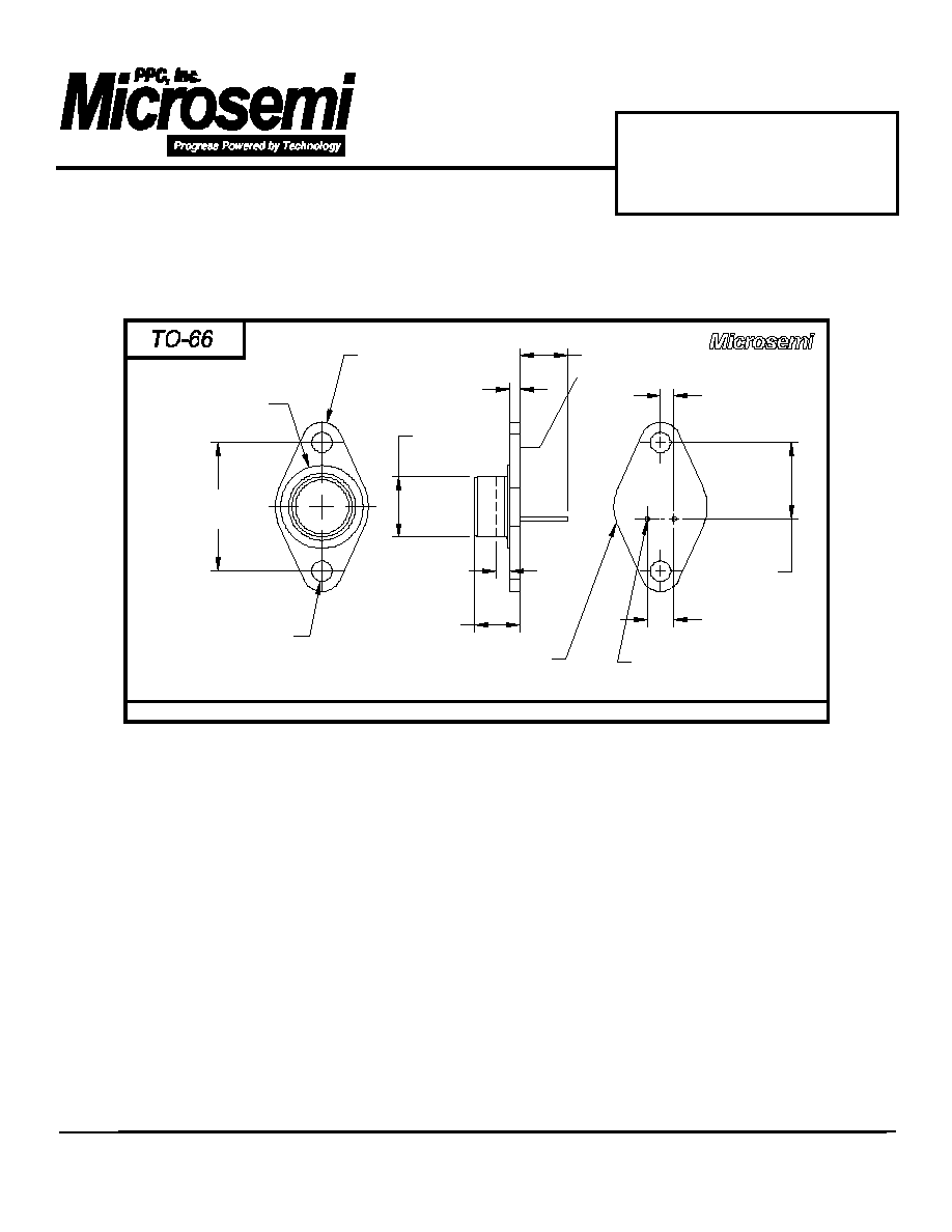
TO-66
APPLICATIONS:
∑
Drivers
∑
Switches
∑
Medium-Power Amplifiers
7516 Central Industrial Drive
Riviera Beach, Florida
33404
PHONE: (561) 842-0305
FAX: (561) 845-7813
DESCRIPTION:
DESCRIPTION:
These power transistors are produced by PPC's DOUBLE
DIFFUSED PLANAR process. This technology produces high
voltage devices with excellent switching speeds, frequency
response, gain linearity, saturation voltages, high current gain,
and safe operating areas. They are intended for use in
Commercial, Industrial, and Military power switching, amplifier,
and regulator applications.
Ultrasonically bonded leads and controlled die mount
techniques are utilized to further increase the SOA capability
and inherent reliability of these devices. The temperature
range to 200
∞∞
C permits reliable operation in high ambients, and
the hermetically sealed package insures maximum reliability
and long life.
*
Indicates JEDEC registered data.
FEATURES:
∑
Low Saturation Voltage: 0.6 V
CE(sat)
@ I
C
= 1.0 Amp
∑
High Gain Characteristics:
hFE @ I
C
= 250 mA: 30-100
∑
Excellent Safe Area Limits
∑
Complementary to NPN 2N3766 (2N3740)

MSC1039.PDF 03-12-99
2N3740
ELECTRICAL CHARACTERISTICS:
ELECTRICAL CHARACTERISTICS:
(25
∞∞
Case Temperature Unless Otherwise Noted)
VALUE
SYMBOL
CHARACTERISTIC
TEST CONDITIONS
Min.
Max.
Units
V
CEO(sus)*
Collector-Emitter
Sustaining Voltage
I
C
= 100 mAdc, I
B
= 0 (Note 1)
60
----
Vdc
I
EB0*
Emitter Base Cutoff
Current
V
EB
= 7.0 Vdc
----
0.5
mAdc
I
CEX*
Collector Cutoff Current
V
CE
= 60 Vdc, V
BE(off)
= 1.5 Vdc
V
CE
= 40 Vdc, V
BE(off)
= 1.5 Vdc, T
C
= 150
∞∞
C
----
----
100
1.0
µ
µ
Adc
mAdc
I
CEO
*
Collector-Emitter Cutoff
Current
V
CE
= 40 Vdc, I
B
= 0
----
1.0
mAdc
I
CBO*
Collector Base Cutoff
Current
V
CB
= 60 Vdc, I
E
= 0
----
100
µ
µ
Adc
h
FE
*
DC Current Gain
(Note 1)
I
C
= 100 mAdc, V
CE
= 1.0 Vdc
I
C
= 250 mAdc, V
CE
= 1.0 Vdc
I
C
= 500 mAdc, V
CE
= 1.0 Vdc
I
C
= 1.0 Adc, V
CE
= 1.0 Vdc
40
30
20
10
----
100
----
----
----
----
----
----
V
CE(sat)
*
Collector-Emitter
Saturation Voltage
(Note 1)
I
C
= 1.0 Adc, I
B
= 125 mAdc
----
0.6
Vdc
V
BE*
Base-Emitter Voltage
(Note 1)
I
C
= 250 mAdc, V
CE
= 1.0 Vdc
----
1.0
Vdc
f
T
*
Current Gain Bandwidth
Product
I
C
= 100 mAdc, V
CE
= 10 Vdc, f = 1.0 MHz
3.0
----
MHz
h
fe
*
Small-Signal Current
Gain
I
C
= 50 mAdc, V
CE
= 10 Vdc, f = 1.0 kHz
25
----
----
C
ob*
Common Base Output
Capacitance
V
CB
= 10 Vdc, I
C
= 0, f = 100 kHz
----
100
pF
Note 1: Pulse Test: PW
300
µ
µ
s, Duty Cycle
2.0%
* Indicates JEDEC registered data.