TECHNICAL DATA
NPN POWER SWITCHING SILICON TRANSISTOR
Qualified per MIL-PRF-19500/374
Devices
Qualified Level
2N3996
2N3997
2N3998
2N3999
JAN
JANTX
JANTXV
MAXIMUM RATINGS
Ratings
Symbol
Value
Unit
Collector-Emitter Voltage
V
CEO
80
Vdc
Collector-Base Voltage
V
CBO
100
Vdc
Emitter-Base Voltage
V
EBO
8.0
Vdc
Base Current
I
B
0.5
Adc
Collector Current
I
C
5.0
10
(1)
Adc
Total Power Dissipation @ T
A
= +25
0
C
(2)
@ T
C
= +100
0
C
(3)
P
T
2.0
30
W
Operating & Storage Junction Temperature Range
T
J,
T
stg
-65 to +200
0
C
THERMAL CHARACTERISTICS
Characteristics
Symbol
Max.
Unit
Thermal Resistance, Junction-to-Case
R
JC
3.33
0
C/W
1) This value applies for t
p
1.0 ms, duty cycle
50%
2) Derate linearly 11.4 mW/
0
C for T
A
> +25
0
C
3) Derate linearly 300 mW/
0
C for T
C
> +100
0
C
*See appendix A for
package outline
ELECTRICAL CHARACTERISTICS (T
C
= 25
0
C unless otherwise noted)
Characteristics
Symbol
Min.
Max.
Unit
OFF CHARACTERISTICS
Collector-Emitter Breakdown Voltage
I
C
= 50 mAdc
V
(BR)CEO
80
Vdc
Collector-Emitter Breakdown Voltage
I
C
= 10
µ
Adc
V
(BR)CBO
100
Vdc
Collector-Emitter Cutoff Current
V
CE
= 60 Vdc
I
CEO
10
µ
Adc
Collector-Emitter Cutoff Current
V
CE
= 80 Vdc, V
BE
= 0
I
CES
200
Adc
Emitter-Base Cutoff Current
V
EB
= 5.0 Vdc
V
EB
= 8.0 Vdc
I
EBO
200
10
Adc
µ
Adc
6 Lake Street, Lawrence, MA 01841
1-800-446-1158 / (978) 794-1666 / Fax: (978) 689-0803
120101
Page 1 of 2
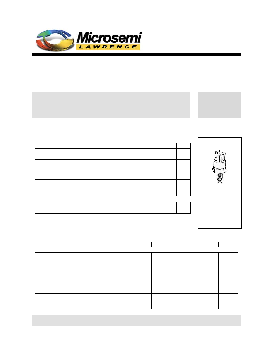
TO-111*
2N3996, 2N3997, 2N3998, 2N3999 JAN SERIES
ELECTRICAL CHARACTERISTICS (con't)
Characteristics
Symbol
Min.
Max.
Unit
ON CHARACTERISTICS
(4)
Forward-Current Transfer Ratio
I
C
= 50 mAdc, V
CE
= 2.0 Vdc 2N3996, 2N3998
I
C
= 1.0 Adc, V
CE
= 2.0 Vdc
I
C
= 5.0 Adc, V
CE
= 5.0 Vdc
I
C
= 50 mAdc, V
CE
= 2.0 Vdc 2N3997, 2N3999
I
C
= 1.0 Adc, V
CE
= 2.0 Vdc
I
C
= 5.0 Adc, V
CE
= 5.0 Vdc
h
FE
30
40
15
60
80
20
120
240
Collector-Emitter Saturation Voltage
I
C
= 1.0 Adc, I
B
= 0.1 Adc
I
C
= 5.0 Adc, I
B
= 0.5 Adc
V
CE(sat)
0.25
2.0
Vdc
Base-Emitter Saturation Voltage
I
C
= 1.0 Adc, I
B
= 0.1 Adc
I
C
= 5.0 Adc, I
B
= 0.5 Adc
V
BE(sat)
0.6
1.2
1.6
Vdc
DYNAMIC CHARACTERISTICS
Magnitude of Common Emitter Small-Signal Short-Circuit
Forward Current Transfer Ratio
I
C
= 1.0 Adc, V
CE
= 5.0 Vdc, f = 10 MHz
h
fe
3.0
12
Output Capacitance
V
CB
= 10 Vdc, I
E
= 0, 100 kHz
f
1.0 MHz
C
obo
150
pF
SAFE OPERATING AREA
DC Tests
T
C
= 100
0
C, 1 Cycle, t = 1.0 s
Test 1
V
CE
= 80 Vdc, I
C
= 0.08 Adc
Test 2
V
CE
= 20 Vdc, I
C
= 1.5 Adc
(4) Pulse Test: Pulse Width = 300
µ
s, Duty Cycle
2.0%.
6 Lake Street, Lawrence, MA 01841
1-800-446-1158 / (978) 794-1666 / Fax: (978) 689-0803
120101
Page 2 of 2