MSC1058.PDF 05-19-99
2N4240
ABSOLUTE MAXIMUM RATINGS:
ABSOLUTE MAXIMUM RATINGS:
SYMBOL
CHARACTERISTIC
VALUE
UNITS
V
CBO
*
Collector-Base Voltage
500
Volts
V
CEO
*
Collector-Emitter Voltage
300
Volts
V
CER
*
Collector-Emitter Voltage R
BE
= 50
400
Volts
V
EBO
*
Emitter-Base Voltage
6
Volts
I
C
*
Peak Collector Current
5
Amps
I
C
*
Continuous Collector Current
2
Amps
I
B
*
Base Current
1
Amps
T
STG
*
Storage Temperature
-65 to 200
∞∞
C
T
J
*
Operating Junction Temperature
-65 to 200
∞∞
C
*
Lead Temperature 1/16" from Case for 10 Sec.
235
∞∞
C
P
T
*
JC
Power Dissipation
T
C
= 25
∞∞
C
Thermal Impedance
35
5.0
Watts
∞∞
C/W
5 Amp, 500V,
High Voltage
NPN Silicon Power
Transistors
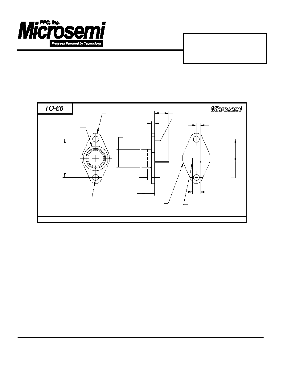
TO-66
APPLICATIONS:
∑
Off-Line Inverters
∑
Deflection Circuits
∑
Switching Regulators
∑
DC-DC Converters
∑
Motor Controls
∑
High Voltage Amplifiers
7516 Central Industrial Drive
Riviera Beach, Florida
33404
PHONE: (561) 842-0305
FAX: (561) 845-7813
DESCRIPTION:
DESCRIPTION:
These power transistors are produced by PPC's DOUBLE
DIFFUSED PLANAR process. This technology produces high
voltage devices with excellent switching speeds, frequency
response, gain linearity, saturation voltages, high current gain,
and safe operating areas. They are intended for use in
Commercial, Industrial, and Military power switching, amplifier,
and regulator applications.
Ultrasonically bonded leads and controlled die mount
techniques are utilized to further increase the SOA capability
and inherent reliability of these devices. The temperature
range to 200
∞∞
C permits reliable operation in high ambients, and
the hermetically sealed package insures maximum reliability
and long life.
*
Indicates JEDEC registered data.
FEATURES:
∑
High Voltage: 250 to 500V
∑
High Current: 2 Amps
∑
Fast Switching: t
f
< 3
µ
µ
sec.
∑
Low V
CE (SAT)
∑
High Power: 35 Watts
MSC1058.PDF 05-19-99
2N4240
ELECTRICAL CHARACTERISTICS:
ELECTRICAL CHARACTERISTICS:
(25
∞∞
Case Temperature Unless Otherwise Noted)
VALUE
SYMBOL
CHARACTERISTIC
TEST CONDITIONS
Min.
Max.
Units
V
CEO(sus)
*
Collector-Emitter
Sustaining Voltage
I
C
= 0.2 Amp (Notes
Ë
Ë
and 2)
300
----
Volts
V
CER(sus)
Collector-Emitter
Sustaining Voltage
I
C
= 0.2A, R
BE
= 50
(Notes 1 and 2)
400
----
Volts
I
CEV*
Collector Cutoff Current
V
CE
= 450V, V
BE
= -1.5V
----
2.0
mA.
I
CEV
*
Collector Cutoff Current
T
C
= 150
∞∞
C
V
CE
= 300V, V
BE
= -1.5V
----
5.0
mA.
I
CEO*
Collector Cutoff Current
V
CE
= 150V, I
B
= 0
----
5.0
mA.
I
EB0*
Emitter Cutoff Current
V
EB
= 6V, I
C
= 0
----
0.5
mA.
h
FE
*
DC Forward Current
Transfer Ratio
(Note 1)
I
C
= 0.1A, V
CE
= 10V
I
C
= 0.75A, V
CE
= 10V
I
C
= 0.75A, V
CE
= 2V
40
30
10
----
150
100
----
----
----
V
CE(sat)
*
Collector-Emitter
Saturation Voltage
(Note 1)
I
C
= 0.75A, I
B
= .075A
----
1.0
Volts
V
BE(sat)
*
Base-Emitter Saturation
Voltage (Note 1)
I
C
= 0.75A, I
B
= .075A
----
1.8
Volts
I
S/b
Second-Breakdown
Collector Current (with
base forward biased)
V
CE
= 100V, t = 1.0sec.
0.35
----
A
E
S/b
Second-Breakdown
Energy (with base
reverse biased)
V
EB
= 4V, R
BE
= 20
, L = 100
µ
µ
h
50
----
µ
µ
J
h
fe
*
Common-Emitter Small-
Signal Forward Current
Transfer Ratio
V
CE
= 10V, I
C
= 0.2A, f = 5 MHz
3
----
----
I
h
fe
I*
Common-Emitter Small-
Signal Forward Current
Transfer Ratio, f = 5 MHz
V
CE
= 10V, I
C
= 0.2A
3.0
----
----
C
Ob
Collector-Base
Capacitance
V
CB
= 10V, I
E
= 0, f = 1.0MHz
----
120
pf
tr*
Rise Time
I
C
= .75A, I
B2
= .075A
----
.05
µ
µ
sec.
ts*
Storage Time
I
C
= .75A, I
B1
= I
B2
= .075A
----
6.0
µ
µ
sec.
tf*
Fall Time
I
C
= .75A, I
B1
= I
B2
= .075A
----
3.0
µ
µ
sec.
Note 1: Pulse Test: Pulse width = 300
µ
µ
Sec., Rep. Rate 60Hz.
Note 2: Caution - Do not use Curve Tracer.
* Indicates JEDEC registered data.