
SG109/SG309
4/90 Rev 1.1 2/94
L
INFINITY
Microelectronics Inc.
Copyright
©
1994
11861 Western Avenue
Garden Grove, CA 92841
1
(714) 898-8121
FAX: (714) 893-2570
FEATURES
∑∑
∑∑
∑
Fully compatible with TTL and DTL
∑∑
∑∑
∑
Output current in excess of 1A
∑∑
∑∑
∑
Internal thermal overload protection
∑∑
∑∑
∑
No additional external components
∑∑
∑∑
∑
Bandgap reference voltage
∑∑
∑∑
∑
Foldback current limiting
HIGH RELIABILITY FEATURES-SG109
Available to MIL-STD-883
MIL - M38510 / 10701BXA - JAN109T
Radiation data available
LMI level "S" processing available
5 -VOLT FIXED VOLTAGE REGULATORS
DESCRIPTION
The SG109/SG309 is a completely self-contained 5V regulator.
Designed to provide local regualtion at currents up to 1A for digital
logic cards, this device is available in the hermetic TO-3, TO-66, TO-
39 and hermetic and plastic TO-220.
A major feature of the SG109's design is its built-in protective
features which make it essentially blowout proof. These consist of
both current limiting to control the peak currents and thermal
shutdown to protect against excessive power dissipation. With the
only added component being a possible need for an input bypass
capacitor, this regulator becomes extremely easy to apply. Utilizing
an improved Bandgap reference design, problems have been
eliminated that are normally associated with the zener diode
references, such as drift in output voltage and large changes in the
line and load regulation.
SCHEMATIC

SG109/SG309
4/90 Rev 1.1 2/94
L
INFINITY
Microelectronics Inc.
Copyright
©
1994
11861 Western Avenue
Garden Grove, CA 92841
2
(714) 898-8121
FAX: (714) 893-2570
Input Voltage ........................................................................ 35V
Power Dissipation ........................................... Internally Limited
Storage Temperature Range ............................. -65
∞
C to 150
∞
C
ABSOLUTE MAXIMUM RATINGS
(Note 1)
Note 1. Exceeding these ratings could cause damage to the device.
K Package:
Thermal Resistance-
Junction to Case
,
JC
................. 3.0∞C/W
Thermal Resistance-
Junction to Ambient
,
JA
.............. 35∞C/W
R Package:
Thermal Resistance-
Junction to Case
,
JC
................. 5.0∞C/W
Thermal Resistance-
Junction to Ambient
,
JA
.............. 40∞C/W
IG Package:
Thermal Resistance-
Junction to Case
,
JC
................. 3.5∞C/W
Thermal Resistance-
Junction to Ambient
,
JA
.............. 42∞C/W
T Package:
Thermal Resistance-
Junction to Case
,
JC
.................. 15∞C/W
Thermal Resistance-
Junction to Ambient
,
JA
............. 120∞C/W
THERMAL DATA
Input Voltage Range ............................................... 7.0V to 25V
Note 2. Range over which the device is functional.
ELECTRICAL CHARACTERISTICS
(Unless otherwise specified, these specifications apply over the operating ambient temperatures for SG109 with -55∞C
T
A
150∞C, SG309 with
0∞C
T
A
125∞C, and for V
IN
= 10V, I
OUT
= 500mA (K, R, and IG -Power Packages-) and I
OUT
= 100mA (T-package). Low duty cycle pulse testing techniques
are used which maintains junction and case temperatures equal to the ambient temperature.)
RECOMMENDED OPERATING CONDITIONS
(Note 2)
Units
SG309
SG109
Parameter
Test Conditions
T
A
= 25∞C
V
IN
= 7.1V to 25V, T
A
= 25∞C
T
A
= 25∞C
Power Pkgs: I
OUT
= 5mA to 1.5A
T-package: I
OUT
=5mA to 500mA
V
IN
= 7.4V to 25V
Power Pkgs: I
OUT
= 5mA to 1.0A,
P
20W
T-package: I
OUT
=5mA to 200mA, P
20W
V
IN
= 7.4V to 25V
With Line : V
IN
= 7.4V to 25V
With Load: Power Pkgs: I
OUT
= 5mA to 1.0A
T-package: I
OUT
=5mA to 200mA
f = 10Hz to 100KHz, T
A
= 25∞C
T
A
= 25∞C
Output Voltage
Line Regulation
Load Regulation
Total Output Voltage Tolerance
Quiescent Current
Quiescent Current Change
Output Noise Voltage
Long Term Stability
Ripple Rejection
4.7
4.6
4.6
50
5.05
4.0
15
15
5.0
5.0
40
10
5.3
50
100
50
5.4
5.4
10
0.5
0.8
0.8
4.8
4.75
4.75
50
5.05
4.0
15
15
5.00
5.00
40
20
5.2
50
100
50
5.25
5.25
10
0.5
0.8
0.8
V
mV
mV
mV
V
V
mA
mA
mA
mA
µV
mV
dB
Min.
Max.
Typ.
Min.
Typ. Max.
Operating Junction Temperature Range
SG109 ............................................................ -55∞C to 150∞C
SG309 ............................................................... 0∞C to 125∞C
Operating Junction Temperature
Hermetic (K, R, T, IG-Packages) .................................. 150
∞
C
Lead Temperature (Soldering, 10 Seconds) ................ 300
∞
C
Note A. Junction Temperature Calculation: T
J
= T
A
+ (P
D
x
JA
).
Note B. The above numbers for
JC
are maximums for the limiting
thermal resistance of the package in a standard mount-
ing configuration. The
JA
numbers are meant to be
guidelines for the thermal performance of the device/
pc-board system. All of the above assume no ambient
airflow.
SG109/SG309
4/90 Rev 1.1 2/94
L
INFINITY
Microelectronics Inc.
Copyright
©
1994
11861 Western Avenue
Garden Grove, CA 92841
3
(714) 898-8121
FAX: (714) 893-2570
Note 1. Contact factory for JAN and DESC product availability.
2. All parts are viewed from the top.
3. Product is also available in leadless chip carrier (LCC) and hermetic flat pack (F).
Contact factory for price and availability.
CONNECTION DIAGRAMS & ORDERING INFORMATION
(See Notes Below)
Ambient
Temperature Range
Part No.
Package
Connection Diagram
3-TERMINAL TO-3
METAL CAN
K-PACKAGE
SG109K/883B
-55∞C to 125∞C
SG109K
-55∞C to 125∞C
SG309K
0∞C to 70∞C
2
1
CASE IS GROUND
3-TERMINAL TO-66
METAL CAN
R-PACKAGE
SG109R/883B
-55∞C to 125∞C
SG109R
-55∞C to 125∞C
SG309R
0∞C to 70∞C
1
2
CASE IS GROUND
GROUND
3-PIN TO-39 METAL CAN
T-PACKAGE
SG109T/883B
-55∞C to 125∞C
JAN109T
-55∞C to 125∞C
SG109T
-55∞C to 125∞C
SG309T
0∞C to 70∞C
GROUND
3
2
1
TAB
IS
GROUND
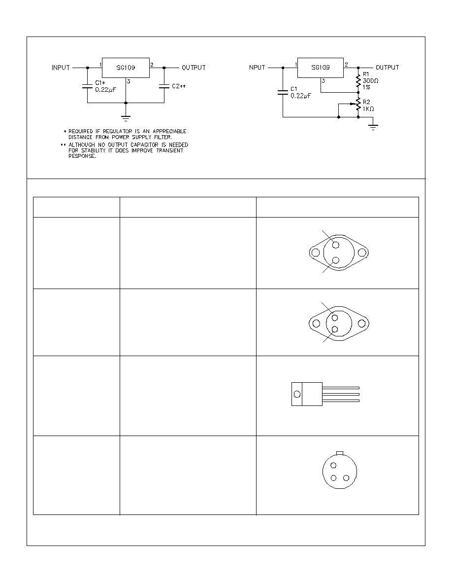
APPLICATION CIRCUITS
FIGURE 1 - FIXED 5V REGULATOR
FIGURE 2 - ADJUSTABLE OUTPUT REGULATOR
V
IN
V
OUT
V
IN
V
OUT
V
IN
V
OUT
V
IN
V
OUT
3-PIN HERMETIC TO-257
IG-PACKAGE (Isolated)
SG109IG/883B
-55∞C to 125∞C
SG109IG
-55∞C to 125∞C