 | –≠–ª–µ–∫—Ç—Ä–æ–Ω–Ω—ã–π –∫–æ–º–ø–æ–Ω–µ–Ω—Ç: JAN1526BJ | –°–∫–∞—á–∞—Ç—å:  PDF PDF  ZIP ZIP |
4/90 Rev 1.1 2/94
L
INFINITY
Microelectronics Inc.
Copyright
©
1994
11861 Western Avenue
Garden Grove, CA 92841
1
(714) 898-8121
FAX: (714) 893-2570
SG1526B/SG2526B/SG3526B
DESCRIPTION
The SG1526B is a high-performance pulse width modulator for switching
power supplies which offers improved functional and electrical characteris-
tics over the industry-standard SG1526. A direct pin-for-pin replacement for
the earlier device with all its features, it incorporates the following enhance-
ments: a bandgap reference circuit for improved regulation and drift
characteristics, improved undervoltage lockout, lower temperature coeffi-
cients on oscillator frequency and current-sense threshold, tighter toler-
ance on softstart time, much faster SHUTDOWN response, improved
double-pulse supperession logic for higher speed operation, and an im-
proved output driver design with low shoot-through current, and faster rise
and fall times. This versatile device can be used to implement single-ended
or push-pull switching regulators of either polarity, both transformer-less
and transformer-coupled. The SG1526B is specified for operation over the
full military ambient temperature range of -55
∞
C to 150
∞
C. The SG2526B
is characterized for the industrial range of -25
∞
C to 150
∞
C, and the SG3526B
is designed for the commercial range of 0
∞
C to 125
∞
C.
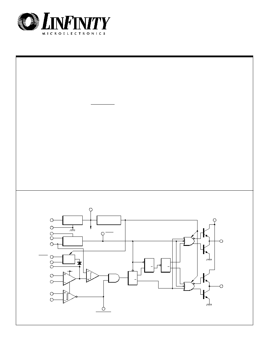
REGULATING PULSE WIDTH MODULATOR
BLOCK DIAGRAM
+V
IN
METERING
F/F
TOGGLE
F/F
MEMORY
F/F
R
D
R
T
C
T
GROUND
Oscillator
Reference
Regulator
Undervoltage
Lockout
Soft
Start
RESET
C
SOFTSTART
COMPENSATION
+ ERROR
-- ERROR
+ C.S.
-- C.S.
SHUTDOWN
Q
Q
Q
Q
OUTPUT B
+V
C
OUTPUT A
+V
IN
FEATURES
∑∑
∑∑
∑
8 to 35 volt operation
∑∑
∑∑
∑
5V low drift 1% bandgap reference
∑∑
∑∑
∑
1Hz to 500KHz oscillator range
∑∑
∑∑
∑
Dual 100mA source/sink
∑∑
∑∑
∑
Digital current limiting
∑∑
∑∑
∑
Double pulse suppression
∑∑
∑∑
∑
Programmable deadtime
∑∑
∑∑
∑
Improved undervoltage lockout
∑∑
∑∑
∑
Single pulse metering
∑∑
∑∑
∑
Programmable soft-start
∑∑
∑∑
∑
Wide current limit common mode range
∑∑
∑∑
∑
TTL/CMOS compatible logic ports
∑∑
∑∑
∑
Symmetry correction capability
∑∑
∑∑
∑
Guaranteed 6 unit synchronization
∑∑
∑∑
∑
Shoot thru currents less than 100mA
∑∑
∑∑
∑
Improved shutdown delay
∑∑
∑∑
∑
Improved rise and fall time
HIGH RELIABILITY FEATURES - SG1526B
Available to MIL-STD-883
MIL-M38510/12603BVA - JAN1526BJ
Radiation data available
LMI level "S" processing available
Amp
V
REF
To Internal
Circuitry
SYNC
S
R
D
S
T
Q
4/90 Rev 1.1 2/94
L
INFINITY
Microelectronics Inc.
Copyright
©
1994
11861 Western Avenue
Garden Grove, CA 92841
2
(714) 898-8121
FAX: (714) 893-2570
SG1526B/SG2526B/SG3526B
ABSOLUTE MAXIMUM RATINGS
(Note 1)
(Note 1)
40V
40V
-0.3V to 5.5V
-0.3V to V
IN
200mA
50mA
Input Voltage (V
IN
) ...............................................................
Collector Supply Voltage (V
C
) .............................................
Logic Inputs .........................................................
Analog Inputs ..........................................................
Source/Sink Load Current (each output) .......................
Reference Load Current ..................................................
Logic Sink Current ...........................................................
Operating Junction Temperature
Hermetic (J, L Packages) .............................................
Plastic (N, DW Packages) ............................................
Storage Temperature Range ............................
Lead Temperature (Soldering, 10 Seconds) ...................
15mA
150
∞
C
150
∞
C
-65
∞
C to 150
∞
C
300
∞
C
Note 1. Exceeding these ratings could cause damage to the device.
THERMAL DATA
J Package:
Thermal Resistance-
Junction to Case
,
JC
.................. 25∞C/W
Thermal Resistance-
Junction to Ambient
,
JA
.............. 70∞C/W
N Package:
Thermal Resistance-
Junction to Case
,
JC
.................. 30∞C/W
Thermal Resistance-
Junction to Ambient
,
JA
............. 60∞C/W
DW Package:
Thermal Resistance-
Junction to Case
,
JC
.................. 35∞C/W
Thermal Resistance-
Junction to Ambient
,
JA
............. 90∞C/W
L Package:
Thermal Resistance-
Junction to Case
,
JC
................... 35∞C/W
Thermal Resistance-
Junction to Ambient
,
JA
........... 120∞C/W
Note A. Junction Temperature Calculation: T
J
= T
A
+ (P
D
x
JA
).
Note B. The above numbers for
JC
are maximums for the limiting
thermal resistance of the package in a standard mount-
ing configuration. The
JA
numbers are meant to be
guidelines for the thermal performance of the device/pc-
board system. All of the above assume no ambient
airflow.
RECOMMENDED OPERATING CONDITIONS
(Note 2)
Input Voltage .............................................................
Collector Supply Voltage ........................................
Sink/Source Load Current (each output) ................
Reference Load Current ...........................................
Oscillator Frequency Range ..............................
Oscillator Timing Resistor ..................................
8V to 35V
4.5V to 35V
0 to 100mA
0 to 20mA
1Hz to 500KHz
2K
to 150K
Oscillator Timing Capacitor ...............................
Available Deadtime Range at 40KHz ......................
Operating Junction Temperature Range:
SG1526B .......................................................
SG2526B .........................................................
SG3526B ............................................................
470pF to 20
µ
F
5% to 50%
-55
∞
C to 125
∞
C
-25
∞
C to 85
∞
C
0
∞
C to 70
∞
C
Note 2. Range over which the device is functional.
ELECTRICAL CHARACTERISTICS
(Unless otherwise specified, these specifications apply over the operating ambient temperatures for SG1526B with -55
∞
C
T
A
125
∞
C, SG2526B with
-25
∞
C
T
A
85
∞
C, SG3526B with 0
∞
C
T
A
70
∞
C, and V
IN
= 15V. Low duty cycle pulse testing techniques are used which maintains junction and
case temperatures equal to the ambient temperature.)
Reference Section
(Note 3)
T
J
= 25
∞
C
V
IN
= 8 to 35V
I
L
= 0 to 20mA
Over Operating T
J
V
REF
= 0V
Output Voltage
Line Regulation
Load Regulation
Temperature Stability
(Note 9)
Total Output Voltage Range
(Note 9)
Short Circuit Current
SG3526B
Units
Undervoltage Lockout Section
V
REF
= 3.8V
V
REF
= 4.8V
RESET Output Voltage
RESET Output Voltage
Parameter
Test Conditions
4.95
4.90
25
5.00
7
10
15
5.00
50
SG1526B/2526B
2.4
0.2
4.8
0.4
Min. Typ. Max. Min. Typ. Max.
5.05
10
20
50
5.10
125
4.90
4.85
25
5.00
10
10
15
5.00
50
5.10
20
25
50
5.15
125
V
mV
mV
mV
V
mA
2.4
0.2
4.8
0.4
V
V
4/90 Rev 1.1 2/94
L
INFINITY
Microelectronics Inc.
Copyright
©
1994
11861 Western Avenue
Garden Grove, CA 92841
3
(714) 898-8121
FAX: (714) 893-2570
SG1526B/SG2526B/SG3526B
R
S
50
mV
µ
A
ns
I
SOURCE
= 40
µ
A
I
SINK
= 3.6mA
V
IH
= 2.4V
V
IL
= 0.4V
(Note9)
2.4
2.4
4
0.2
-125
-225
0.4
-200
-360
200
4
0.2
-125
-225
0.4
-200
-360
200
V
V
µ
A
µ
A
ns
Minimum Duty Cycle
Maximum Duty Cycle
V
COMPENSATION
= 0.4V
V
COMPENSATION
= 3.6V
45
49
0
45
49
0
%
%
I
SOURCE
= 20mA
I
SOURCE
= 100mA
I
SINK
= 20mA
I
SINK
= 100mA
V
C
= 40V
C
L
= 1000pF
C
L
= 1000pF
HIGH Output Voltage
LOW Output Voltage
Collector Leakage
Rise Time
Fall Time
R
S
2K
R
L
10M
V
PIN1
- V
PIN2
150mV, I
SOURCE
= 100
µ
A
V
PIN2
- V
PIN1
150mV, I
SINK
= 100
µ
A
R
S
2K
V
IN
= 8V to 35V
Error Amplifier Section
(Note 5)
Input Offset Voltage
Input Bias Current
Input Offset Current
DC Open Loop Gain
High Output Voltage
Low Output Voltage
Common Mode Rejection
Supply Voltage Rejection
Oscillator Section
(Note 4)
T
J
= 25
∞
C
V
IN
= 8 to 35V
Over Operating T
J
R
T
= 150K
, C
T
= 20
µ
F
R
T
= 2K
, C
T
= 470pF
V
IN
= 35V
V
IN
= 8V
R
L
= 2.0K
to V
REF
Initial Accuracy
Voltage Stability
Temperature Stability
(Note 9)
Minimum Frequency
(Note 9)
Maximum Frequency
Sawtooth Peak Voltage
Sawtooth Valley Voltage
SYNC Pulse Width
SG3526B
Test Conditions
Parameter
Units
RESET = 0.4V
RESET = 2.4V
Error Clamp Voltage
C
S
Charging Current
ELECTRICAL CHARACTERISTICS
(continued)
Soft-Start Section
Note 3. I
L
= 0mA
Note 4. F
OSC
= 40KHz (R
T
= 4.12K
±
1%, C
T
= .01
µ
F
±
1%, R
D
= 0
)
Note 5. V
CM
= 0 to 5.2V
Note 6. V
CM
= 0 to 12V
Note 7. V
C
= 15V
Note 8. V
IN
= 35V
Note 9. These parameters, although guaranteed over the recom-
mended operating conditions, are not tested in production.
Standby Current
0.3
2
150
0.4
0.15
5
-1000
100
0.4
±
8
1.0
10
1.0
3.5
1.1
2
SG1526B/2526B
0.4.
150
Min. Typ. Max. Min. Typ. Max.
500
2.5
0.5
±
3
0.5
7
3.0
1.0
1.0
500
2.5
0.5
±
3
0.5
3
3.0
1.0
1.0
±
8
1.0
5
1.0
3.5
1.1
2
%
%
%
Hz
KHz
V
V
µ
s
64
3.6
70
66
2
-350
35
72
4.2
0.2
94
80
60
3.6
70
66
2
-350
35
72
4.2
0.2
94
80
10
-2000
200
0.4
mV
nA
nA
dB
V
V
dB
dB
PWM Comparator Section
(Note 4)
Digital Ports (SYNC, SHUTDOWN, and RESET)
HIGH Output Voltage
LOW Output Voltage
HIGH Input Current
LOW Input Current
SHUTDOWN Delay to Output
Current Limit Comparator Section
(Note 6)
Sense Voltage
Input Bias Current
Delay to Output
(Note 9)
120
-10
400
100
-3
80
110
-10
400
100
-3
90
Output Drivers (each output)
(Note 7)
50
0.1
100
50
0.1
100
0.4.
150
V
µ
A
V
V
V
V
µ
A
µ
s
µ
s
0.3
2
150
0.4
0.15
13.5
13
0.2
1.2
50
0.3
0.1
12.5
12
13.5
13
0.2
1.2
50
0.3
0.1
12.5
12
Power Consumption Section
(Note 8)
SHUTDOWN = 0.4V
18
30
18
30
mA
4/90 Rev 1.1 2/94
L
INFINITY
Microelectronics Inc.
Copyright
©
1994
11861 Western Avenue
Garden Grove, CA 92841
4
(714) 898-8121
FAX: (714) 893-2570
SG1526B/SG2526B/SG3526B
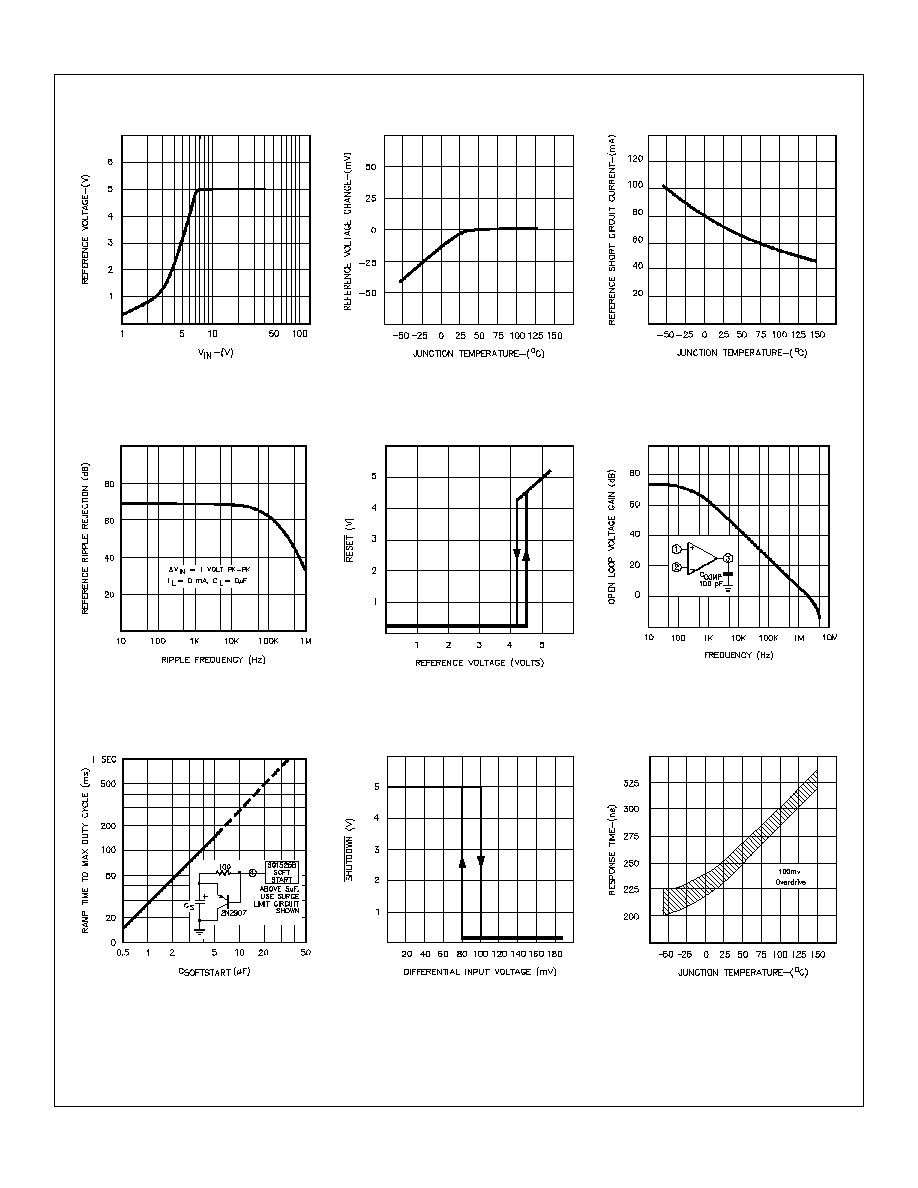
FIGURE 1.
REFERENCE VOLTAGE VS. SUPPLY VOLTAGE
FIGURE 3.
REFERENCE SHORT CIRCUIT
FIGURE 2.
REFERENCE TEMPERATURE STABILITY
FIGURE 6.
ERROR AMPLIFIER OPEN LOOP GAIN
VS. FREQUENCY
FIGURE 5.
UNDER VOLTAGE LOCKOUT
FIGURE 7.
SOFTSTART TIME CONSTANT VS. C
S
FIGURE 9.
COMPARATOR INPUT TO DRIVER OUTPUT DELAY
FIGURE 8.
CURRENT LIMIT TRANSFER FUNCTION
CHARACTERISTIC CURVES
FIGURE 4.
REFERENCE RIPPLE REJECTION
4/90 Rev 1.1 2/94
L
INFINITY
Microelectronics Inc.
Copyright
©
1994
11861 Western Avenue
Garden Grove, CA 92841
5
(714) 898-8121
FAX: (714) 893-2570
SG1526B/SG2526B/SG3526B
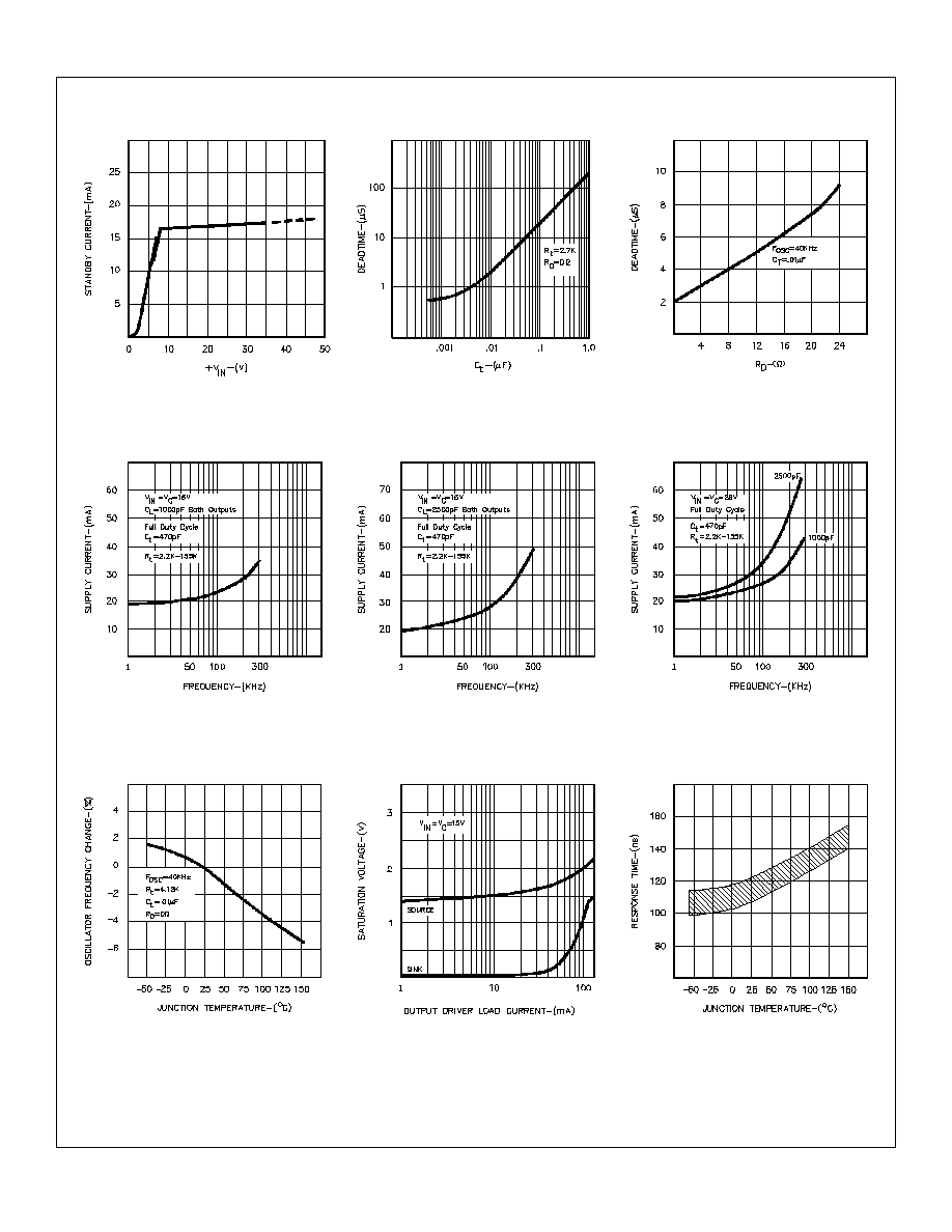
FIGURE 10.
STANDBY CURRENT VS. SUPPLY VOLTAGE
FIGURE 12.
OUTPUT DRIVER DEADTIME VS. R
D
VALUE
FIGURE 11.
OUTPUT DRIVER DEADTIME VS. C
T
VALUE
FIGURE 15.
SUPPLY CURRENT VS. OUTPUT FREQUENCY
FIGURE 14.
SUPPLY CURRENT VS. OUTPUT FREQUENCY
FIGURE 16.
OSCILLATOR FREQUENCY
TEMPERATURE STABILITY
FIGURE 18.
SHUTDOWN INPUT TO DRIVER OUTPUT DELAY
FIGURE 17.
OUTPUT DRIVER SATURATION VOLTAGE
CHARACTERISTIC CURVES
(continued)
FIGURE 13.
SUPPLY CURRENT VS. OUTPUT FREQUENCY