1 Watt Metal Case Zener Diodes
S C O T T S D A L E D I V I S I O N
1N3821 thru 1N3830A
W
W
W
.
Mi
c
r
o
s
e
m
i
.
C
O
M
1N3821 ≠ 1N3830A
DESCRIPTION
APPEARANCE
This well established zener diode series for the 1N3821 thru 1N3830A
JEDEC registration in the glass hermetic sealed DO-13 package provides a
low voltage selection for 3.3 to 7.5 volts. It is also well suited for high-
reliability applications where it is available in JAN, JANTX, and JANTXV
military qualifications. Higher voltages are also available in the 1N3016
thru 1N3051 series (6.8 V to 200 V) in the same package (see separate
data sheet). Microsemi also offers numerous other Zener diode products
for a variety of other packages including surface mount.
DO-13
(DO-202AA)
IMPORTANT: For the most current data, consult MICROSEMI's website:
http://www.microsemi.com
FEATURES
APPLICATIONS / BENEFITS
∑ Zener Voltage Range: 3.3 V to 7.5 V
∑ Hermetically sealed DO-13 metal package
∑ Internally solder-bonded construction.
∑ Also available in JAN, JANTX, JANTXV
qualifications per MIL-PRF19500/115 by adding the
JAN, JANTX, or JANTXV prefixes to part numbers
for desired level of screening, e.g. JANTX1N3821,
JANTXV1N3051A, etc.
∑ Surface mount also available with 1N3821UR-1
thru 1N30330AUR-1 series on separate data sheet
∑
Regulates voltage over a broad operating current
and temperature range
∑
Low voltage selection from 3.3 to 7.5 V
∑
Tight voltage tolerances available
∑
Low reverse (leakage) currents
∑
Nonsensitive to ESD
∑
Hermetically sealed metal package
∑
Inherently radiation hard as described in Microsemi
MicroNote 050
MAXIMUM RATINGS
MECHANICAL AND PACKAGING
∑ Operating Junction and Storage Temperatures:
-65
o
C to +175
o
C
∑ THERMAL RESISTANCE: 50
o
C/W* junction to lead
at 0.375 inches (10 mm) from body or 110
o
C/W
junction to ambient when leads are mounted on FR4
PC board with 4 mm
2
copper pads (1 oz) and track
width 1 mm, length 25 mm
∑ DC Power Dissipation
*
: 1 Watt at T
L
< +125
o
C 3/8"
(10 mm) from body or 1.0 Watts at T
L
< +65
o
C when
mounted on FR4 PC board as described for thermal
resistance above (also see Fig 1)
∑ Forward Voltage @ 200 mA: 1.5 Volts.
∑ Solder Temperatures: 260
o
C for 10 s (maximum)
∑
CASE: DO-13 (DO-202AA), welded, hermetically
sealed metal and glass
∑
FINISH: All external surfaces are Tin-Lead (Pb/Sn)
plated and solderable per MIL-STD-750 method
2026
∑
POLARITY: Cathode connected case.
∑
WEIGHT: 1.4 grams.
∑
Tape & Reel option: Standard per EIA-296 (add
"TR" suffix to part number)
∑
See package dimensions on last page
* For further mounting reference, thermal resistance from junction to metal case may be reduced to
<
20
o
C/W
when mounting DO-13 metal case directly on heat sink.
Microsemi
Scottsdale Division
8700 E. Thomas Rd. PO Box 1390, Scottsdale, AZ 85252 USA, (480) 941-6300, Fax: (480) 947-1503
Page 1
Copyright
2003
11-06-2003 REV A
1 Watt Metal Case Zener Diodes
S C O T T S D A L E D I V I S I O N
1N3821 thru 1N3830A
W
W
W
.
Mi
c
r
o
s
e
m
i
.
C
O
M
1N3821 ≠ 1N3830A
*ELECTRICAL CHARACTERISTICS @ 25
o
C
MAXIMUM ZENER IMPEDANCE
(Note 2)
NOMINAL
ZENER
VOLTAGE
V
Z
@ I
ZT
(Note 1)
ZENER
TEST
CURRENT
I
ZT
Z
ZT
@ I
ZT
Z
ZK
@ I
ZK
= 1mA
MAXIMUM
ZENER
CURRENT
I
ZM
(Note 3)
MAXIMUM
REVERSE
LEAKAGE
CURRENT
I
R
@ V
R
TYPICAL
TEMP. COEFF.
OF ZENER
VOLTAGE
VZ
JEDEC
TYPE
NUMBER
Volts mA OHMS OHMS
mA
µA
Volts
%/
o
C
1N3821
1N3821A
1N3822
1N3822A
3.3
3.3
3.6
3.6
76
76
69
69
10
10
10
10
400
400
400
400
276
276
252
252
100
100
100
100
1
1
1
1
-.066
-.066
-.058
-.058
1N3823
1N3823A
1N3824
1N3824A
3.9
3.9
4.3
4.3
64
64
58
58
9
9
9
9
400
400
400
400
238
238
213
213
50
50
10
10
1
1
1
1
-.046
-.046
-.033
-.033
1N3825
1N3825A
1N3826
1N3826A
4.7
4.7
5.1
5.1
53
53
49
49
8
8
7
7
500
500
550
550
194
194
178
178
10
10
10
10
1
1
1
1
-.015
-.015
+/-.010
+/-.010
1N3827
1N3827A
1N3828
1N3828A
5.6
5.6
6.2
6.2
45
45
41
41
5
5
2
2
600
600
700
700
162
162
146
146
10
10
10
10
2
2
3
3
+.030
+.030
+.049
+.049
1N3829
1N3829A
1N3830
1N3830A
6.8
6.8
7.5
7.5
37
37
34
34
1.5
1.5
1.5
1.5
500
500
250
250
133
133
121
121
10
10
10
10
3
3
3
3
+.053
+.053
+.057
+.057
*JEDEC Registered Data.
NOTES: 1. The JEDEC type numbers shown with suffix A have a standard tolerance of +/-5% on the nominal zener voltage. V
Z
measured
with device in thermal equilibrium in 25
o
C still air and mounted in test clips, æ" from unit body. if tighter tolerance on V
Z
is required,
consult
factory.
2.
The zener impedance is derived when a 60 cycle ac current having an rms value equal to 10% of the dc zener current (I
ZT
or I
ZK
) is
superimposed on I
ZT
or I
ZK
. Zener impedance is measured at 2 points to ensure a sharp knee on the breakdown curve and to
eliminate unstable units. See MicroNote 202 for variation in dynamic impedance with different zener currents.
3.
Allowance has been made for the increase in
V
Z
due to Z
Z
and for the increase in junction temperature as the unit approaches
thermal equilibrium at the power dissipation of 1 watt.
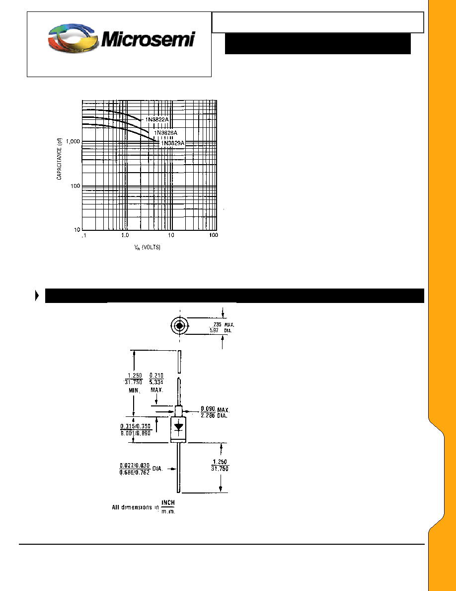
GRAPHS
Rated Po
w
e
r Dissipation (W
)
T
L
T
A
T
L
≠ Lead Temperature (
o
C) 3/8" from body
FIGURE
2
or T
A
on FR4 PC Board
Temperature
Coeff.
vs. Zener Voltage
FIGURE 1
Power Derating
Microsemi
Scottsdale Division
8700 E. Thomas Rd. PO Box 1390, Scottsdale, AZ 85252 USA, (480) 941-6300, Fax: (480) 947-1503
Page 2
Copyright
2003
11-06-2003 REV A