6 Lake Street - Lawrence, MA 01841
Applications
Used in general purpose applications,where a low current controlled forward
characteristic and fast switching speed are important.
Features
Six sigma quality
Metallurgically bonded
BKC's Sigma BondTM plating
for problem free solderability
LL-34/35 MELF SMD available
Full approval to Mil-S-19500/337
Available up to JANTXV-1 levels
"S" level screening available to SCDs
Silicon Switching Diode
DO-35 Glass Package
1N4150
1N4153,
1N4153-1
Maximum Ratings
Symbol
Value
Unit
Peak Inverse Voltage
PIV
75 (Min.)
Volts
Average Rectified Current
I
Avg
150
mAmps
Continuous Forward Current
I
Fdc
300
mAmps
Peak Surge Current (t
peak
= 1 Sec.)
I
peak
0.25
Amp
BKC Power Dissipation T
L
= 50
o
C, L = 3/8" from body
P
tot
500
mWatts
Operating and Storage Temperature Range
T
Op & St
-65 to +200
o
C
Electrical Characteristics @ 25
o
C*
Symbol Minimum Maximum
Unit
Forward Voltage
@ I
F
= 100 �A V
F
Vf
0.49
0.55
Volts
Forward Voltage
@ I
F
= 250 �A V
F
Vf 0.53
0.59
Volts
Forward Voltage
@ I
F
= 1.0 mA V
F
Vf 0.59
0.67
Volts
Forward Voltage
@ I
F
= 2.0 mA V
F
Vf 0.62
0.70
Volts
Forward Voltage
@ I
F
= 10 mA
V
F
0.70
0.81
Volts
Forward Voltage
@ I
F
= 20 mA
V
F
0.74
0.88
Volts
Reverse Leakage Current @ V
R
= 50 V
I
R
0.05(50 @ 150
o
C)
�A
Breakdown Voltage @ I
R
= 5.0 �A
PIV
75
Volts
Capacitance @ V
R
= 0 V, f = 1mHz
C
T
2.0
pF
Reverse Recovery Time (note 1)
t
rr
4.0
nSecs
Reverse Recovery Time (note 2)
t
rr
2.0
nSec
Note 1: Per Method 4031-A with I
F
= I
R
= 10 mA, R
L
= 100 Ohms, C = 3 Pf. *Unless Otherwise Specified
Note2: Per Method 4031-A with I
F
= I
R
= 10 mA, Rr = 6 Volts, Rl=100 ohms.
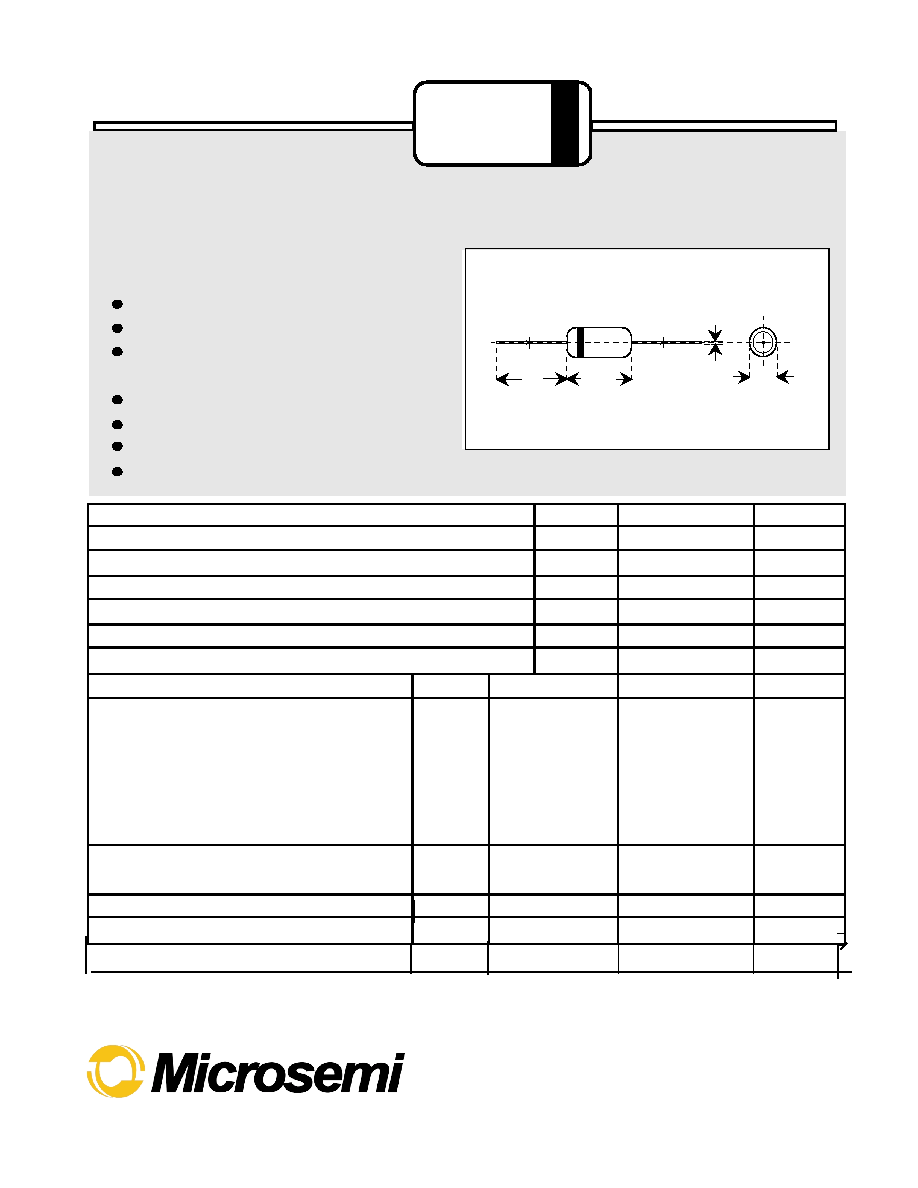
DO-35 Glass Package
Dia.
0.06-0.09"
1.0"
25.4 mm
(Min.)
Length
0.120-.200"
3.05-5.08-
m m
1.53-2.28 m m
0 .0 18-0 .0 22"
0 .458-0 .558 m m
Lea d Di
a .