
Low Voltage Surface Mount
500 mW Avalanche Diodes
S C O T T S D A L E D I V I S I O N
IN5518BUR-1 thru 1N5546BUR-1
(or MLL5518B-1 thru MLL5546B-1)
W
W
W
.
Mi
c
r
o
s
e
m
i
.
C
O
M
1N5
518
BUR �
1N5
546
BUR
DESCRIPTION
APPEARANCE
The 1N5518BUR-1 thru 1N5546BUR-1 series of 0.5 watt glass surface
mount Zener voltage regulators provides a selection from 3.3 to 33 volts in
standard 5% tolerances as well as tighter tolerances identified by different
suffix letters on the part number. These have an internal-metallurgical-bond
option as identified by the "�1" suffix. This internally bonded Zener package
construction is also in JAN, JANTX, and JANTXV military qualifications.
Microsemi also offers numerous other Zener products to meet higher and
lower power applications.
DO-213AA
IMPORTANT: For the most current data, consult MICROSEMI's website:
http://www.microsemi.com
FEATURES
APPLICATIONS / BENEFITS
� Surface mount equivalent to JEDEC registered
1N5518 thru 1N5546 series
� Internal metallurgical bond with the "-1" suffix
� Also available in JAN, JANTX, and JANTXV
qualifications per MIL-PRF-19500/437 by adding
the JAN, JANTX, or JANTXV prefixes to part
numbers for desired level of screening; (e.g.
JANTX1N4099UR-1, JANTXV1N4109CUR-1, etc.)
� Nonbonded types also available without the "-1"
suffix for both the axial and surface mount
packages
� DO-7 or DO-35 glass body axial-leaded Zener
equivalents also available per JEDEC registration
with part numbers 1N5518 thru 1N5546 on
separate data sheets
�
Regulates voltage over a broad operating current
and temperature range
�
Extensive selection from 3.3 to 33 V
�
Standard voltage tolerances are plus/minus 5% with
a "B" suffix, e.g. 1N5518BUR-1, etc.
�
Tight tolerances available in plus or minus 2% or 1%
with C or D suffix respectively, e.g. 1N5518CUR-1,
1N5518DUR-1, etc.
�
Hermetically sealed surface mount package
�
Nonsensitive to ESD per MIL-STD-750 Method 1020
�
Minimal capacitance (see Figure 3)
�
Inherently radiation hard as described in Microsemi
MicroNote 050
MAXIMUM RATINGS
MECHANICAL AND PACKAGING
� Operating and Storage temperature: -65
�
C to
+175
�
C
� Thermal Resistance: 100
�
C/W junction to end cap,
or 250
�
C/W junction to ambient when mounted on
FR4 PC board (1 oz Cu) with recommended
footprint (see last page)
� Steady-State Power: 0.5 watts at end cap
temperature T
EC
< 125
o
C or at ambient T
A
< 50
�
C
when mounted on FR4 PC board as described for
thermal resistance above (see Figure 2 for
derating)
� Forward voltage @200 mA: 1.1 volts
� Solder Temperatures: 260
�
C for 10 s (max)
�
CASE: Hermetically sealed glass DO-213AA
(SOD80 or MLL34) MELF style package
�
TERMINALS: End caps tin-lead plated solderable
per MIL-STD-750, method 2026
�
POLARITY: Cathode indicated by band where
diode is to be operated with the banded end positive
with respect to the opposite end for Zener regulation
�
MARKING: cathode band only
� TAPE & REEL option: Standard per EIA-481-1-A
with 12 mm tape, 2000 per 7 inch reel or 5000 per
13 inch reel (add "TR" suffix to part number)
�
WEIGHT: 0.04 grams
�
See package dimensions on last page
Microsemi
Scottsdale Division
8700 E. Thomas Rd. PO Box 1390, Scottsdale, AZ 85252 USA, (480) 941-6300, Fax: (480) 947-1503
Page 1
Copyright
2003
10-31-2003 REV B
Low Voltage Surface Mount
500 mW Avalanche Diodes
S C O T T S D A L E D I V I S I O N
IN5518BUR-1 thru 1N5546BUR-1
(or MLL5518B-1 thru MLL5546B-1)
W
W
W
.
Mi
c
r
o
s
e
m
i
.
C
O
M
1N5
518
BUR �
1N5
546
BUR
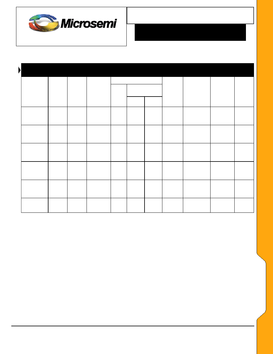
ELECTRICAL CHARACTERISTICS
(T
A
= 25
o
C unless otherwise noted. Based on DC measurements at
thermal equilibrium;
V
F
= 1.1 Max @ IF = 200 mA for all types.)
MAX. REVERSE CURRENT
(Note 4)
V
R
� VOLTS
JEDEC TYPE
NUMBER
(Note 1 and
Note 7)
NOMINAL
ZENER
VOLTAGE
V
Z
@ I
ZT
(Note 2)
VOLTS
TEST
CURRENT
I
ZT
mAdc
MAX. ZENER
IMPEDANCE
B-C-D SUFFIX
Z
ZT
@ I
ZT
(Note 3)
OHMS
I
R
�Adc
NON & A-
SUFFIX
B-C-D
SUFFIX
B-C-D
SUFFIX
MAXIMUM
DC ZENER
CURRENT
I
ZM
(Note 5)
mAdc
B-C-D SUFFIX
MAX. NOISE
DENSITY
AT I
Z
= 250
�A
N
D
�V/ Hz
REGULATION
FACTOR
V
Z
(Note 6)
VOLTS
LOW V
Z
CURRENT
I
ZL
(Note 6)
mAdc
1N5518BUR-1
1N5519BUR-1
1N5520BUR-1
1N5521BUR-1
1N5522BUR-1
3.3
3.6
3.9
4.3
4.7
20
20
20
20
10
26
24
22
18
22
5.0
3.0
1.0
3.0
2.0
0.90
0.90
0.90
1.0
1.5
1.0
1.0
1.0
1.5
2.0
115
105
98
88
81
0.5
0.5
0.5
0.5
0.5
0.90
0.90
0.85
0.75
0.60
2.0
2.0
2.0
2.0
1.0
1N5523BUR-1
1N5524BUR-1
1N5525BUR-1
1N5526BUR-1
1N5527BUR-1
5.1
5.6
6.2
6.8
7.5
5.0
3.0
1.0
1.0
1.0
26
30
30
30
35
2.0
2.0
1.0
1.0
0.5
2.0
3.0
4.5
5.5
6.0
2.5
3.5
5.0
6.2
6.8
75
68
61
56
51
0.5
1.0
1.0
1.0
2.0
0.65
0.30
0.20
0.10
0.05
0.25
0.25
0.01
0.01
0.01
1N5528BUR-1
1N5529BUR-1
1N5530BUR-1
1N5531BUR-1
1N5532BUR-1
8.2
9.1
10.0
11.0
12.0
1.0
1.0
1.0
1.0
1.0
40
45
60
80
90
0.5
0.1
0.05
0.05
0.05
6.5
7.0
8.0
9.0
9.5
7.5
8.2
9.1
9.9
10.8
46
42
38
35
32
4.0
4.0
4.0
5.0
10
0.05
0.05
0.10
0.20
0.20
0.01
0.01
0.01
0.01
0.01
1N5533BUR-1
1N5534BUR-1
1N5535BUR-1
1N5536BUR-1
1N5537BUR-1
13.0
14.0
15.0
16.0
17.0
1.0
1.0
1.0
1.0
1.0
90
100
100
100
100
0.01
0.01
0.01
0.01
0.01
10.5
11.5
12.5
13.0
14.0
11.7
12.6
13.5
14.4
15.3
29
27
25
24
22
15
20
20
20
20
0.20
0.20
0.20
0.20
0.20
0.01
0.01
0.01
0.01
0.01
1N5538BUR-1
1N5539BUR-1
1N5540BUR-1
1N5541BUR-1
1N5542BUR-1
18.0
19.0
20.0
22.0
24.0
1.0
1.0
1.0
1.0
1.0
100
100
100
100
100
0.01
0.01
0.01
0.01
0.01
15.0
16.0
17.0
18.0
20.0
16.2
17.1
18.0
19.8
21.6
21
20
19
17
16
20
20
20
20
20
0.20
0.20
0.20
0.25
0.30
0.01
0.01
0.01
0.01
0.01
1N5543BUR-1
1N5544BUR-1
1N5545BUR-1
1N5546BUR-1
25.0
28.0
30.0
33.0
1.0
1.0
1.0
1.0
100
100
100
100
0.01
0.01
0.01
0.01
21.0
23.0
24.0
28.0
22.4
25.2
27.0
29.7
15
14
13
12
20
20
20
20
0.35
0.40
0.45
0.50
0.01
0.01
0.01
0.01
NOTES:
1.
TOLERANCE AND VOLTAGE DESIGNATION �
The JEDEC type numbers without a letter prior to the UR-1 suffix are +/-20% with guaranteed limits for only V
Z
, I
R
, and V
F
.
Units with "A" prior to the UR-1 suffix are +/-10% with guaranteed limits for V
Z
, I
R
, and V
F
. Units with guaranteed limits for all six
parameters are indicated by a B suffix for +/-5.0% units, C suffix for +/-2.0% and D suffix for +/-1.0% prior to the UR-1 suffix.
2.
ZENER VOLTAGE (V
Z
) MEASUREMENT �
Nominal zener voltage is measured with the device junction in thermal equilibrium with ambient temperature of 25
o
C.
3.
ZENER IMPEDANCE (Z
Z
) MEASUREMENT �
The zener impedance is derived from the 60 Hz ac voltage, which results when an ac current having an rms value equal to 10%
of the dc zener current (I
ZT
) is superimposed on I
ZT
.
4.
REVERSE CURRENT (I
R
) �
Reverse currents are guaranteed and are measured at V
R
as shown on the table.
5.
MAXIMUM REGULATOR CURRENT (I
ZM
) �
The maximum current shown is as shown in MIL-PRF-19500/437.
6.
MAXIMUM REGULATION FACTOR (
V
Z
) �
V
Z
is the maximum difference between V
Z
at I
ZT
and V
Z
at I
ZL
measured with the device junction in thermal equilibrium.
7.
PART NUMBER � These may be ordered as either 1N5518BUR-1 thru 1N5546BUR-1 or as MLL5518B-1 thru MLL5546B-1 part
numbers. For military types, use the 1NxxxUR-1 format and also include JAN, JANTX, or JANTXV prefix for desired screening
level, e.g. JANTX1N5518BUR-1, JANTXV1N5532BUR-1, JANTXV1N5534CUR-1, JANTXV1N5545DUR-1, etc.
Microsemi
Scottsdale Division
8700 E. Thomas Rd. PO Box 1390, Scottsdale, AZ 85252 USA, (480) 941-6300, Fax: (480) 947-1503
Page 2
Copyright
2003
10-31-2003 REV B

Low Voltage Surface Mount
500 mW Avalanche Diodes
Microsemi
Scottsdale Division
8700 E. Thomas Rd. PO Box 1390, Scottsdale, AZ 85252 USA, (480) 941-6300, Fax: (480) 947-1503
Page 3
Copyright
2003
10-31-2003 REV B
W
W
W
.
Mi
c
r
o
s
e
m
i
.
C
O
M
S C O T T S D A L E D I V I S I O N
IN5518BUR-1 thru 1N5546BUR-1
(or MLL5518B-1 thru MLL5546B-1)
1N5
518
BUR �
1N5
546
BUR
GRAPHS and CIRCUIT
Noise density, (N
D
) is specified in
microvolt-rms per square-root-hertz.
Actual measurement is performed
using a 1 kHz to 3 kHz frequency
bandpass filter at a constant Zener test
current (I
ZT
) at 25
o
C ambient
temperature.
P
d
Rated Po
wer
Dissipation (m
W
)
FIGURE
1
Noise Density
Measurement Circuit
T
EC
T
A
T
EC
, End Cap Temperature (
o
C) or T
A
Ambient temperature on FR4 PC board
FIGURE 2 Power Derating Curve
T
y
pical Capacita
n
ce in Picofarads (pf)
Zener Voltage V
Z
FIGURE 4
FIGURE 3
Capacitance vs. Zener Voltage (Typical)
Zener Diode Characteristics and Symbol Identification
PACKAGE DIMENSIONS
INCHES MILLIMETERS
DIM
MIN MAX MIN MAX
A
0.063 0.067 1.60 1.70
B
0.130 0.146 3.30 3.70
C
0.016 0.022 0.41 0.55
PAD LAYOUT
INCHES mm
A
.200 5.08
B
.055 1.40
C
.080 2.03