6 LAKE STREET, LAWRENCE, MASSACHUSETTS 01841
PHONE (978) 620-2600
FAX (978) 689-0803
WEBSITE: http://www.microsemi.com
143
FIGURE 1
DESIGN DATA
CASE: DO-213AA, Hermetically sealed
glass case. (MELF, SOD-80, LL34)
LEAD FINISH: Tin / Lead
THERMAL RESISTANCE: (ROJEC):
100 ∞C/W maximum at L = 0 inch
THERMAL IMPEDANCE: (ZOJX): 35
∞C/W maximum
POLARITY: Diode to be operated with
the banded (cathode) end positive.
MOUNTING SURFACE SELECTION:
The Axial Coefficient of Expansion
(COE) Of this Device is Approximately
+6PPM/∞C. The COE of the Mounting
Surface System Should Be Selected To
Provide A Suitable Match With This
Device.
MAXIMUM RATINGS
Junction and Storage Temperature: -65∞C to +125∞C
DC Power Dissipation: 500 mW @ TEC = +125∞C
Power Derating: 10 mW / ∞C above TEC = +125∞C
Forward Voltage @ 200mA: 1.1 volts maximum
ELECTRICAL CHARACTERISTICS @ 25∞C, unless otherwise specified.
B-C-D
SUFFIX
CDI
NOMINAL
ZENER MAX. ZENER MAXIMUM REVERSE
MAXIMUM
REGULATION
LOW
TYPE
ZENER
TEST
IMPEDANCE
LEAKAGE CURRENT
DC ZENER
FACTOR
VZ
NUMBER
VOLTAGE CURRENT B-C-D SUFFIX
CURRENT
CURRENT
VZ@ 1ZT
1ZT
ZZT @ 1ZT
lR
VR = VOLTS
1ZM
VZ
1ZL
(NOTE 1)
(NOTE 2)
(NOTE 3)
(NOTE 4)
(NOTE 5)
NON & A-
B-C-D-
VOLTS
mA
OHMS
µ
Adc
SUFFIX
SUFFIX
mA
VOLTS
mA
CDLL5518B
3.3
20
26
5.0
0.90
1.0
115
0.90
2.0
CDLL5519B
3.6
20
24
3.0
0.90
1.0
105
0.90
2.0
CDLL5520B
3.9
20
22
1.0
0.90
1.0
98
0.85
2.0
CDLL5521B
4.3
20
18
3.0
1.0
1.5
88
0.75
2.0
CDLL5522B
4.7
10
22
2.0
1.5
2.0
81
0.60
1.0
CDLL5523B
5.1
5.0
26
2.0
2.0
2.5
75
0.65
0.25
CDLL5524B
5.6
3.0
30
2.0
3.0
3.5
68
0.30
0.25
CDLL5525B
6.2
1.0
30
1.0
4.5
5.0
61
0.20
0.01
CDLL5526B
6.8
1.0
30
1.0
5.5
6.2
56
0.10
0.01
CDLL5527B
7.5
1.0
35
0.5
6.0
6.8
51
0.05
0.01
CDLL5528B
8.2
1.0
40
0.5
6.5
7.5
46
0.05
0.01
CDLL5529B
9.1
1.0
45
0.1
7.0
8.2
42
0.05
0.01
CDLL5530B
10.0
1.0
60
0.05
8.0
9.1
38
0.10
0.01
CDLL5531B
11.0
1.0
80
0.05
9.0
9.9
35
0.20
0.01
CDLL5532B
12.0
1.0
90
0.05
9.5
10.8
32
0.20
0.01
CDLL5533B
13.0
1.0
90
0.01
10.5
11.7
29
0.20
0.01
CDLL5534B
14.0
1.0
100
0.01
11.5
12.6
27
0.20
0.01
CDLL5535B
15.0
1.0
100
0.01
12.5
13.5
25
0.20
0.01
CDLL5536B
16.0
1.0
100
0.01
13.0
14.4
24
0.20
0.01
CDLL5537B
17.0
1.0
100
0.01
14.0
15.3
22
0.20
0.01
CDLL5538B
18.0
1.0
100
0.01
15.0
16.2
21
0.20
0.01
CDLL5539B
19.0
1.0
100
0.01
16.0
17.1
20
0.20
0.01
CDLL5540B
20.0
1.0
100
0.01
17.0
18.0
19
0.20
0.01
CDLL5541B
22.0
1.0
100
0.01
18.0
19.8
17
0.25
0.01
CDLL5542B
24.0
1.0
100
0.01
20.0
21.6
16
0.30
0.01
CDLL5543B
25.0
1.0
100
0.01
21.0
22.4
15
0.35
0.01
CDLL5544B
28.0
1.0
100
0.01
23.0
25.2
14
0.40
0.01
CDLL5545B
30.0
1.0
100
0.01
24.0
27.0
13
0.45
0.01
CDLL5546B
33.0
1.0
100
0.01
28.0
29.7
12
0.50
0.01
NOTE 1
No Suffix type numbers are +20% with guaranteed limits for only VZ, lR, and VF.
Units with "A" suffix are +10% with guaranteed limits for VZ, lR, and VF. Units with
guaranteed limits for all six parameters are indicated by a "B" suffix for +5.0% units,
"C" suffix for+2.0% and "D" suffix for +1.0%.
NOTE 2
Zener voltage is measured with the device junction in thermal equilibrium at an ambient
temperature of 25∞C + 3∞C.
NOTE 3
Zener impedance is derived by superimposing on 1ZT A 60Hz rms a.c. current equal to
10% of1ZT.
NOTE 4
Reverse leakage currents are measured at VR as shown on the table.
NOTE 5
VZ is the maximum difference between VZ at lZT and VZ at lZL measured
with the device junction in thermal equilibrium.
∑ 1N5518BUR-1 THRU 1N5546BUR-1 AVAILABLE IN
JAN, JANTX AND JANTXV
PER MIL-PRF-19500/437
∑ ZENER DIODE, 500mW
∑ LEADLESS PACKAGE FOR SURFACE MOUNT
∑ LOW REVERSE LEAKAGE CHARACTERISTICS
∑ METALLURGICALLY BONDED
1N5518BUR-1
thru
1N5546BUR-1
and
CDLL5518 thru CDLL5546D
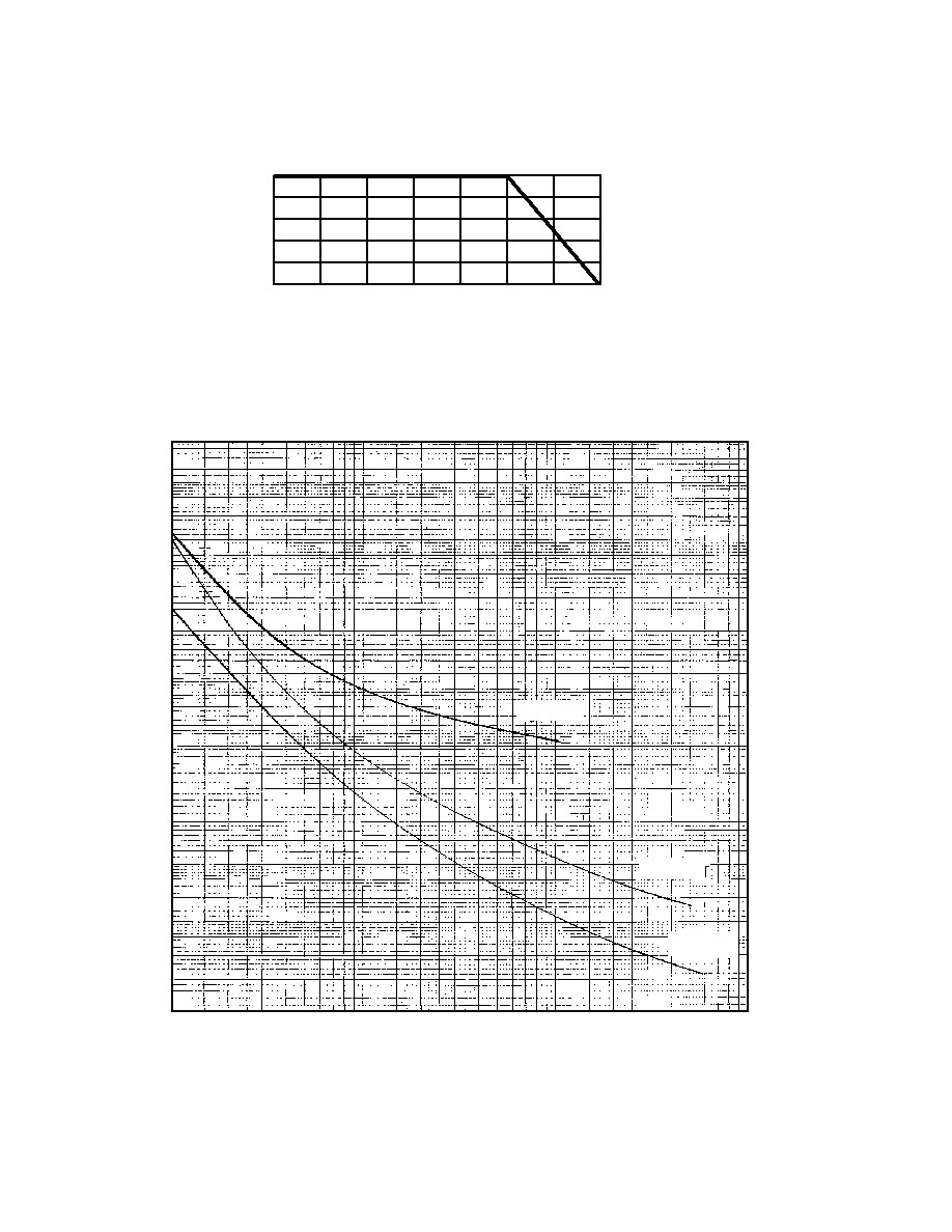
MILLIMETERS INCHES
DIM
MIN
MAX
MIN MAX
D
1.60
1.70
0.063 0.067
F
0.41
0.55
0.016 0.022
G
3.30
3.70
.130 .146
G1
2.54 REF.
.100 REF.
S
0.03 MIN.
.001 MIN.