
Silicon 500 mW Zener Diodes
Microsemi
Scottsdale Division
8700 E. Thomas Rd. PO Box 1390, Scottsdale, AZ 85252 USA, (480) 941-6300, Fax: (480) 947-1503
Page 1
Copyright
2003
10-31-2003 REV B
W
W
W
.
Mi
c
r
o
s
e
m
i
.
C
O
M
S C O T T S D A L E D I V I S I O N
1N957B, -1 thru 1N992B, -1 DO-35
1
N
9
5
7
B
≠
9
9
2
B
(
D
O
-
3
5
)
DESCRIPTION
APPEARANCE
The popular 1N957B thru 1N992B series of 0.5 watt Zener Voltage
Regulators provides a selection from 6.8 to 200 volts in standard 5% or
10% tolerances as well as tighter tolerances identified by different suffix
letters on the part number. These glass axial-leaded DO-35 Zeners are
also available with an internal-metallurgical-bond option by adding a "-1"
suffix. The 1N962B-1 thru 1N992B-1 are available in JAN, JANTX, and
JANTXV military qualifications. Microsemi also offers numerous other
Zener products to meet higher and lower power applications.
DO-35
(DO-204AH)
IMPORTANT: For the most current data, consult MICROSEMI's website:
http://www.microsemi.com
FEATURES
APPLICATIONS / BENEFITS
∑ JEDEC registered 1N957B(-1) to 1N992B(-1) series
∑ Internal metallurgical bond option available by
adding a "-1" suffix
∑ Also available in JAN, JANTX, and JANTXV
qualifications per MIL-PRF-19500/117 by adding the
JAN, JANTX, or JANTXV prefixes to part numbers
for desired level of screening as well as "-1" suffix;
(e.g. JANTX1N962B-1, JANTXV1N986C-1, etc.)
∑ Military Surface Mount equivalents also available in
DO-213AA by adding a UR-1 suffix in addition to the
JAN, JANTX, and JANTXV prefix; e.g.
JANTX1N962BUR-1 (see separate data sheet)
∑ Commercial Surface Mount equivalents available as
MLL957B to MLL992B or with "-1" suffix for bonded
in the DO-213AA MELF style package (consult
factory for others)
∑ DO-7 glass body axial-leaded Zener equivalents are
also available
∑
Regulates voltage over a broad operating
current and temperature range
∑
Extensive selection from 6.8 to 200 V
∑
Standard voltage tolerances are plus/minus 5%
with B suffix, 10 % with A suffix identification
∑
Tight tolerances available in plus or minus 2%
or 1% with C or D suffix respectively
∑
Flexible axial-lead mounting terminals
∑
Nonsensitive to ESD per MIL-STD-750 Method
1020
∑
Minimal capacitance (see Figure 3)
∑
Inherently radiation hard as described in
Microsemi MicroNote 050
MAXIMUM RATINGS
MECHANICAL AND PACKAGING
∑ Operating and Storage temperature: -65
∫
C to
+175
∫
C
∑ Thermal Resistance: 250
∫
C/W junction to lead at 3/8
(10 mm) lead length from body, or 310
∫
C/W junction
to ambient when mounted on FR4 PC board (1 oz
Cu) with 4 mm
2
copper pads and track width 1 mm,
length 25 mm
∑ Steady-State Power: 0.5 watts at T
L
< 50
o
C 3/8 inch
(10 mm) from body or 0.48 W at T
A
< 25
∫
C when
mounted on FR4 PC board as described for thermal
resistance above (also see Figure1)
∑ Forward voltage @200 mA: 1.1 volts (maximum) for
1N957B ≠ 1N985B and 1.3 V for 1N985 ≠ 1N992B
∑ Solder Temperatures: 260
∫
C for 10 s (max)
∑
CASE: Hermetically sealed axial-lead glass
DO-35 (DO-204AH) package
∑
TERMINALS: Leads, tin-lead plated solderable
per MIL-STD-750, method 2026
∑
POLARITY: Cathode indicated by band. Diode
to be operated with the banded end positive
with respect to the opposite end for Zener
regulation
∑
MARKING: Part number
∑
TAPE & REEL option: Standard per EIA-296
(add "TR" suffix to part number)
∑
WEIGHT: 0.2 grams
∑
See package dimensions on last page

Silicon 500 mW Zener Diodes
S C O T T S D A L E D I V I S I O N
1N957B, -1 thru 1N992B, -1 DO-35
W
W
W
.
Mi
c
r
o
s
e
m
i
.
C
O
M
1
N
9
5
7
B
≠
9
9
2
B
(
D
O
-
3
5
)
ELECTRICAL CHARACTERISTICS* @ 25
o
C
NOMINAL
ZENER
VOLTAGE
(Note 2)
V
Z
ZENER
TEST
CURRENT
I
ZT
MAX. ZENER IMPEDANCE
(Note 3)
Z
ZT
@ I
ZT
Z
ZK
@ I
ZK
MAX. DC
ZENER
CURRENT
(Note 4)
I
ZM
MAX. SURGE
CURRENT
(Note 5)
I
ZSM
MAX. REVERSE
LEAKAGE
CURRENT
I
R
@
V
R
MAX. TEMP.
COEFFICIENT
VZ
JEDEC
TYPE
NUMBER
(Note 1)
VOLTS mA OHMS
OHMS
mA mA
mA µA
VOLTS %/
o
C
1N957B
1N958B
1N959B
1N960B
1N961B
6.8
7.5
8.2
9.1
10
18.5
16.5
15.0
14.0
12.5
4.5
5.5
6.5
7.5
8.5
700
700
700
700
700
1.0
.5
.5
.5
.25
55
50
45
41
38
300
275
250
225
200
150
75
50
25
10
5.2
5.7
6.2
6.9
7.6
+0.05
+0.058
+0.065
+0.068
+0.075
1N962B
1N963B
1N964B
1N965B
1N966B
11
12
13
15
16
11.5
10.5
9.5
8.5
7.8
9.5
11.5
13.0
16
17
700
700
700
700
700
.25
.25
.25
.25
.25
32
31
28
25
24
175
160
150
130
120
5
5
5
5
5
8.4
9.1
9.9
11.4
12.2
+0.076
+0.077
+0.079
+0.082
+0.083
1N967B
1N968B
1N969B
1N970B
1N971B
18
20
22
24
27
7.0
6.2
5.6
5.2
4.6
21
25
29
33
41
750
750
750
750
750
.25
.25
.25
.25
.25
20
18
16
15
13
110
100
90
80
70
5
5
5
5
5
13.7
15.2
16.7
18.2
20.6
+0.085
+0.086
+0.087
+0.088
+0.090
1N972B
1N973B
1N974B
1N975B
1N976B
30
33
36
39
43
4.2
3.8
3.4
3.2
3.0
49
58
70
80
93
1000
1000
1000
1000
1500
.25
.25
.25
.25
.25
12
11
10
9.5
8.8
65
60
55
46
44
5
5
5
5
5
22.8
25.1
27.4
29.7
32.7
+0.091
+0.092
+0.093
+0.094
+0.095
1N977B
1N978B
1N979B
1N980B
1N981B
47
51
56
62
68
2.7
2.5
2.2
2.0
1.8
105
125
150
185
230
1500
1500
2000
2000
2000
.25
.25
.25
.25
.25
7.9
7.4
6.8
6.0
5.5
40
37
35
30
28
5
5
5
5
5
35.8
38.8
42.6
47.1
51.7
+0.095
+0.096
+0.096
+0.097
+0.097
1N982B
1N983B
1N984B
1N985B
1N986B
75
82
91
100
110
1.7
1.5
1.4
1.3
1.1
270
330
400
500
750
2000
3000
3000
3000
4000
.25
.25
.25
.25
.25
5.0
4.6
4.1
3.7
3.3
26
23
21
18
16
5
5
5
5
5
56.0
62.2
69.2
76.0
83.6
+0.098
+0.098
+0.099
+0.11
+0.11
1N987B
1N988B
1N989B
1N990B
1N991B
1N992B
120
130
150
160
180
200
1.0
0.95
0.85
0.80
0.68
0.65
900
1100
1500
1700
2200
2500
4500
5000
6000
6500
7100
8000
.25
.25
.25
.25
.25
.25
3.1
2.7
2.4
2.2
2.0
1.8
15
13
12
11
10
9
5
5
5
5
5
5
91.2
98.8
114.0
121.6
136.8
152.0
+0.11
+0.11
+0.11
+0.11
+0.11
+0.11
* JEDEC Registered Data
NOTE 1: The JEDEC type numbers shown (B suffix) have a +/-5% tolerance on nominal Zener voltage. The suffix A is used to identify +/-
10% tolerance; suffix C is used to identify +/-2%; and suffix D is used to identify +/-1% tolerance; no suffix indicates +/-20%
tolerance.
NOTE 2: Zener voltage (
V
Z
) is measured after the test current has been applied for 20 +/- 5 seconds. The device shall be suspended by its
leads with the inside edge of the mounting clips between .375" and .500" from the body. Mounting clips shall be maintained at a
temperature of 25 +8/ -2
o
C.
NOTE 3: The zener impedance is derived when a 60 cycle ac current having an rms value equal to 10% of the dc zener current (I
ZT
or
I
ZK
) is superimposed on I
ZT
or I
ZK
. Zener impedance is measured at 2 points to ensure a sharp knee on the breakdown curve
and to eliminate unstable units. See MicroNote 202 for variation in dynamic impedance with different zener currents.
NOTE 4: The values of
I
ZM
are calculated for a +/- 5% tolerance on nominal zener voltage. Allowance has been made for the rise in zener
voltage above V
ZT
which results from zener impedance and the increase in junction temperature as power dissipation approaches
400 mW. In the case of individual diodes I
ZM
is that value of current which results in a dissipation of 400 mW at 75
o
C lead
temperature at 3/8" from body.
NOTE 5: The surge for I
ZSM
is a square wave or equivalent half-sine wave pulse of 1/120 sec. duration.
Microsemi
Scottsdale Division
8700 E. Thomas Rd. PO Box 1390, Scottsdale, AZ 85252 USA, (480) 941-6300, Fax: (480) 947-1503
Page 2
Copyright
2003
10-31-2003 REV B
Silicon 500 mW Zener Diodes
Microsemi
Scottsdale Division
8700 E. Thomas Rd. PO Box 1390, Scottsdale, AZ 85252 USA, (480) 941-6300, Fax: (480) 947-1503
Page 3
Copyright
2003
10-31-2003 REV B
W
W
W
.
Mi
c
r
o
s
e
m
i
.
C
O
M
S C O T T S D A L E D I V I S I O N
1N957B, -1 thru 1N992B, -1 DO-35
1
N
9
5
7
B
≠
9
9
2
B
(
D
O
-
3
5
)
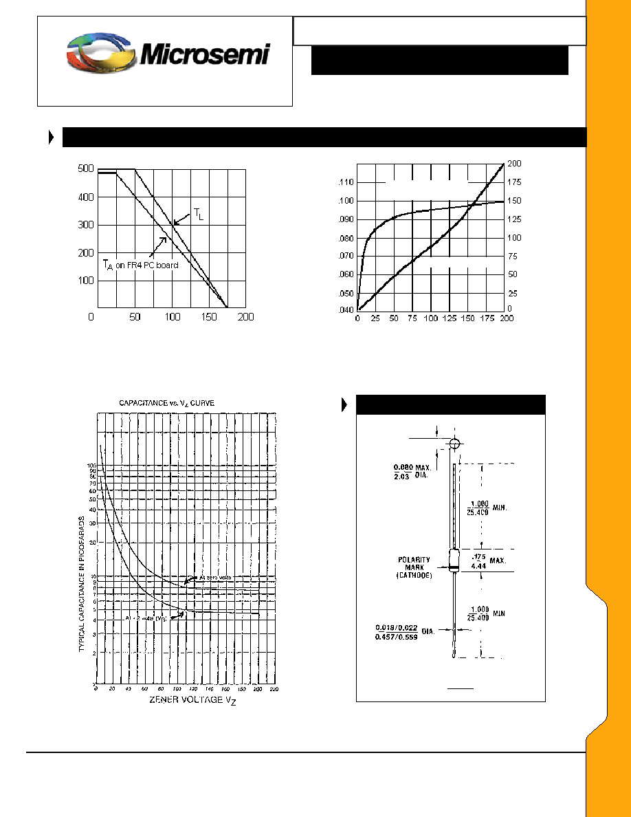
GRAPHS
RATED P
O
W
E
R DISSIPATION -
mW
T
E
M
P
E
R
A
T
U
R
E
C
O
E
F
F
I
C
I
E
N
T
m
V
/
o
C
TEMPERATURE CO
EFFICIENT
%/
o
C
Voltage Temperature
Coefficient %/
o
C
mV Change /∫C
T
L
≠ LEAD TEMPERATURE (
o
C) 3/8" FROM BODY or
NOMINAL ZENER VOLTAGE (VOLTS)
T
A
on FR4 PC BOARD
FIGURE
1
FIGURE
2
POWER DERATING CURVE
ZENER VOLTAGE TEMPERATURE
COEFFICIENT vs. ZENER VOLTAGE
PACKAGE DIMENSIONS
All dimensions in: INCH
mm
FIGURE
3
CAPACITANCE vs. ZENER VOLTAGE
(TYPICAL)