TECHNICAL DATA
PNP SWITCHING SILICON TRANSISTOR
Qualified per MIL-PRF-19500/396
Devices
Qualified Level
2N3762
2N3762L
2N3763
2N3763L
2N3764
2N3765
JAN
JANTX
JANTXV
MAXIMUM RATINGS
Ratings
Symbol
2N3762*
2N3764
2N3763*
2N3765
Unit
Collector-Emitter Voltage
V
CEO
40
60
Vdc
Collector-Base Voltage
V
CBO
40
60
Vdc
Emitter-Base Voltage
V
EBO
5.0
Vdc
Collector Current
I
C
1.5
Adc
2N3762*
1
2N3763*
2N3764
2
2N3765
Total Power Dissipation @ T
A
= +25
0
C
P
T
1.0
0.5
W
Operating & Storage Junction Temp. Range T
op,
T
stg
-55 to +200
0
C
THERMAL CHARACTERISTICS
Characteristics
Symbol
Max.
Unit
2N3762*
2N3763*
2N3764
2N3765
Thermal Resistance Junction-to-Case
R
JC
60
88
0
C/W
*Electrical characteristics for "L" suffix devices are identical to the "non L" corresponding devices
1) Derate linearly at 5.71 mW/
0
C for T
A
> +25
0
C
2) Derate linearly at 2.86 mW/
0
C for T
A
> +25
0
C
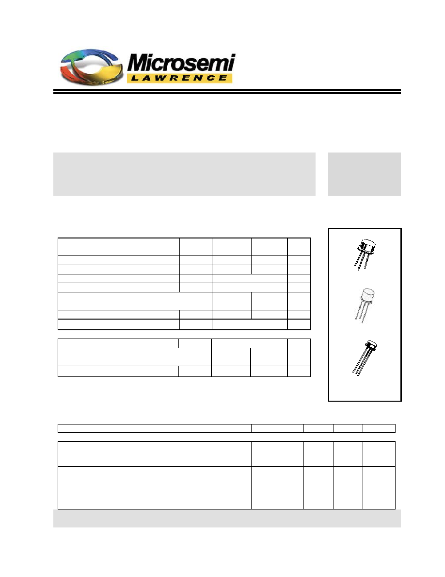
TO-39* (TO-205AD)
2N3762, 2N3763
TO-5*
2N3762L, 2N3763L
TO-46* (TO-206AB)
2N3764, 2N3765
*See appendix A for
package outline
ELECTRICAL CHARACTERISTICS (T
A
= 25
0
C unless otherwise noted)
Characteristics
Symbol
Min.
Max.
Unit
OFF CHARACTERISTICS
Collector-Emitter Breakdown Current
I
C
= 10 mAdc 2N3762, 2N3764
2N3763, 2N3765
V
(BR)CEO
40
60
Vdc
Collector-Base Cutoff Current
V
CB
= 20 Vdc 2N3762, 2N3764
V
CB
= 30 Vdc 2N3763, 2N3765
V
CB
= 40 Vdc 2N3762, 2N3764
V
CB
= 60 Vdc 2N3763, 2N3765
I
CBO
100
100
10
10
Adc
µ
Adc
6 Lake Street, Lawrence, MA 01841
1-800-446-1158 / (978) 794-1666 / Fax: (978) 689-0803
120101
Page 1 of 2
2N3762, L, 2N3763, L, 2N3764, 2N3765 JAN SERIES
ELECTRICAL CHARACTERISTICS (con't)
Characteristics
Symbol
Min.
Max.
Unit
Collector-Emitter Cutoff Current
V
EB
= 2.0 Vdc, V
CE
= 20 Vdc 2N3762, 2N3764
V
EB
= 2.0 Vdc, V
CE
= 30 Vdc 2N3763, 2N3765
I
CEX
100
100
Adc
Emitter-Base Cutoff Current
V
EB
= 2.0 Vdc All Types
V
EB
= 5.0 Vdc 2N3762, 2N3764
2N3763, 2N3765
I
EBO
200
10
10
Adc
µ
Adc
ON CHARACTERISTICS (3)
Forward-Current Transfer Ratio
I
C
= 10 mAdc, V
CE
= 1.0 Vdc
I
C
= 150 mAdc, V
CE
= 1.0 Vdc
I
C
= 500 mAdc, V
CE
= 1.0 Vdc
I
C
= 1.0 Adc, V
CE
= 1.5 Vdc 2N3762, 2N3764
2N3763, 2N3765
I
C
= 1.5 Adc, V
CE
= 5.0 Vdc 2N3762, 2N3764
2N3763, 2N3765
h
FE
35
40
40
30
20
30
20
140
120
80
Collector-Emitter Saturation Voltage
I
C
= 10 mAdc, I
B
= 1.0 mAdc
I
C
= 150 m Adc, I
B
= 15 mAdc
I
C
= 500 mAdc, I
B
= 50 mAdc
I
C
= 1.0 Adc, I
B
= 100 mAdc
V
CE(sat)
0.1
0.22
0.5
0.9
Vdc
Base-Emitter Saturation Voltage
I
C
= 10 mAdc, I
B
= 1.0 mAdc
I
C
= 150 m Adc, I
B
= 15 mAdc
I
C
= 500 mAdc, I
B
= 50 mAdc
I
C
= 1.0 Adc, I
B
= 100 mAdc
V
BE(sat)
0.9
0.8
1.0
1.2
1.4
Vdc
DYNAMIC CHARACTERISTICS
Forward Current Transfer Ratio, Magnitude
I
C
= 50 mAdc, V
CE
= 10 Vdc, f = 100 MHz 2N3762, 2N3764
2N3763, 2N3765
h
fe
1.8
1.5
6.0
6.0
Output Capacitance
V
CB
= 10 Vdc, I
E
= 0, 100 kHz
f
1.0 MHz
C
obo
25
pF
Input Capacitance
V
EB
= 0.5 Vdc, I
C
= 0, 100 kHz
f
1.0 MHz
C
ibo
80
pF
SWITCHING CHARACTERISTICS
Delay Time
V
CC
= 30 Vdc, V
EB
= 0,
t
d
8.0
s
Rise Time
I
C
= 1.0 mAdc, I
B1
= 100 mAdc
t
r
35
s
Storage Time
V
CC
= 30 Vdc, V
EB
= 0,
t
s
80
s
Fall Time
I
C
= 1.0 mAdc, I
B1
= 100 mAdc
t
f
35
s
(3) Pulse Test: Pulse Width = 300
µ
s, Duty Cycle
2.0%.
6 Lake Street, Lawrence, MA 01841
1-800-446-1158 / (978) 794-1666 / Fax: (978) 689-0803
120101
Page 2 of 2