
TECHNICAL DATA
PNP SMALL SIGNAL SILICON TRANSISTOR
Qualified per MIL-PRF-19500/291
Devices
Qualified Level
2N2906A
2N2906AL
2N2906AUA
2N2906AUB
2N2907A
2N2907AL
2N2907AUA
2N2907AUB
JAN
JANTX
JANTXV
JANS
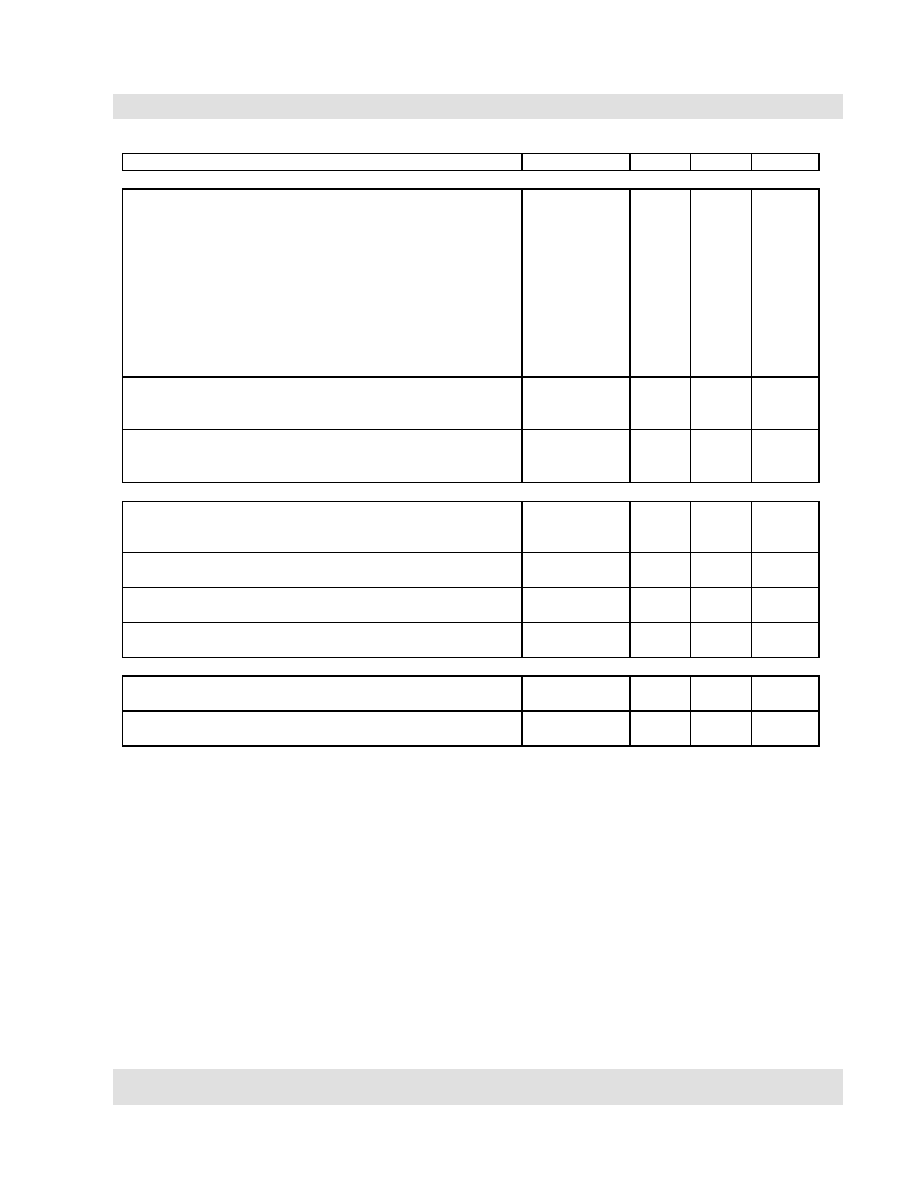
MAXIMUM RATINGS
Ratings
Symbol All Types Unit
Collector-Emitter Voltage
V
CEO
60
Vdc
Collector-Base Voltage
V
CBO
60
Vdc
Emitter-Base Voltage
V
EBO
5.0
Vdc
Collector Current
I
C
600
mAdc
Total Power Dissipation @ T
A
= +25
0
C
@ T
C
= +25
0
C
P
T
(1)
P
T
(2 / 3)
0.4
1.8
W
W
Operating & Storage Junction Temperature Range
T
J,
T
stg
-65 to +200
0
C
1) Derate linearly 2.28 mW/
0
C for T
A
> +25
0
C.
2) Derate linearly 10.3 mW/
0
C for T
C
> +25
0
C.
3) For UA and UB surface mount case outlines: P
T
= 1.16 W;
derate linearly 6.6mW/
0
C for T
C
> +25
0
C.
TO-18* (TO-206AA)
4 PIN*
2N2906AUA, 2N2907AUA
3 PIN*
2N2906AUB, 2N2907AUB
*See appendix A for package outline
ELECTRICAL CHARACTERISTICS (T
A
= 25
0
C unless otherwise noted)
Characteristics
Symbol
Min.
Max.
Unit
OFF CHARACTERISTICS
Collector-Emitter Breakdown Voltage
I
C
= 10 mAdc
V
(BR)CEO
60
Vdc
Collector-Base Cutoff Current
V
CE
= 50 Vdc
V
CE
= 60 Vdc
I
CBO
10
10
µ
Adc
Adc
Collector-Base Cutoff Current
V
CE
= 50 Vdc
I
CES
50
Adc
Emitter-Base Cutoff Current
V
EB
= 4.0 Vdc
V
EB
= 5.0 Vdc
I
EBO
50
10
Adc
µ
Adc
6 Lake Street, Lawrence, MA 01841
1-800-446-1158 / (978) 794-1666 / Fax: (978) 689-0803
120101
Page 1 of 2
2N2906A, 2N2907A JAN SERIES
ELECTRICAL CHARACTERISTICS (con't)
Characteristics
Symbol
Min.
Max.
Unit
ON CHARACTERISTICS
(4)
Forward-Current Transfer Ratio
I
C
= 0.1 mAdc, V
CE
= 10 Vdc 2N2906A. UA, UB
2N2907A, UA, UB
I
C
= 1.0 mAdc, V
CE
= 10 Vdc 2N2906A. UA, UB
2N2907A, UA, UB
I
C
= 10 mAdc, V
CE
= 10 Vdc 2N2906A. UA, UB
2N2907A, UA, UB
I
C
= 150 mAdc, V
CE
= 10 Vdc 2N2906A. UA, UB
2N2907A, UA, UB
I
C
= 500 mAdc, V
CE
= 10 Vdc 2N2906A. UA, UB
2N2907A, UA, UB
h
FE
40
75
40
100
40
100
40
100
40
50
175
450
120
300
Collector-Emitter Saturation Voltage
I
C
= 150 mAdc, I
B
= 15 mAdc
I
C
= 500 mAdc, I
B
= 50 mAdc
V
CE(sat)
0.4
1.6
Vdc
Base-Emitter Saturation Voltage
I
C
= 150 mAdc, I
B
= 15 mAdc
I
C
= 500 mAdc, I
B
= 50 mAdc
V
BE(sat)
0.6
1.3
2.6
Vdc
DYNAMIC CHARACTERISTICS
Forward Current Transfer Ratio
V
CE
= 10 Vdc, I
C
= 1.0 mAdc, f = 1.0 kHz 2N2906A,UA, UB
2N2907A,UA, UB
h
fe
40
100
Magnitude of Small-Signal Forward Current Transfer Ratio
V
CE
= 20 Vdc, I
C
= 20 mAdc, f = 100 MHz
h
fe
2.0
Output Capacitance
V
CB
= 10 Vdc, I
E
= 0, 100 kHz
f
1.0 MHz
C
obo
8.0
pF
Input Capacitance
V
EB
= 2.0 Vdc, I
C
= 0, 100 kHz
f
1.0 MHz
C
ibo
30
pF
SWITCHING CHARACTERISTICS
Turn-On Time
V
CC
= 30 Vdc; I
C
= 150 mAdc; I
B1
=
50 mAdc
t
on
45
s
Turn-Off Time
V
CC
= 30 Vdc; I
C
= 150 mAdc; I
B1
= -
I
B2
=
50 mAdc
t
off
300
s
(4) Pulse Test: Pulse Width = 300
µ
s, Duty Cycle
2.0%.
6 Lake Street, Lawrence, MA 01841
1-800-446-1158 / (978) 794-1666 / Fax: (978) 689-0803
120101
Page 2 of 2