VOIDLESS-HERMETICALLY-SEALED
ULTRAFAST RECOVERY GLASS
RECTIFIERS
S C O T T S D A L E D I V I S I O N
1N5802 thru 1N5806
W
W
W
.
Mi
c
r
o
s
e
m
i
.
C
O
M
1
N
5
8
0
2
�
1
N
5
8
0
6
DESCRIPTION
APPEARANCE
This "ultrafast recovery" rectifier diode series is military qualified to MIL-PRF-
19500/477 and is ideal for high-reliability applications where a failure cannot be
tolerated. These industry-recognized 2.5 Amp rated rectifiers for working peak
reverse voltages from 50 to 150 volts are hermetically sealed with voidless-glass
construction using an internal "Category I" metallurgical bond. They are also
available in surface-mount packages (see separate data sheet for 1N5802US thru
1N5806US). Microsemi also offers numerous other rectifier products to meet higher
and lower current ratings with various recovery time speed requirements including
standard, fast and ultrafast in both through-hole and surface-mount packages.
"A" Package
IMPORTANT: For the most current data, consult MICROSEMI's website:
http://www.microsemi.com
FEATURES
APPLICATIONS / BENEFITS
� Popular JEDEC registered 1N5802 to 1N5806 series
� Voidless hermetically sealed glass package
� Extremely robust construction
� Triple-layer passivation
� Internal "Category I" Metallurgical bonds
� JAN, JANTX, JANTXV, and JANS available per MIL-PRF-
19500/477
� Surface mount equivalents also available in a square end-cap
MELF configuration with "US" suffix (see separate data sheet
for 1N5802US thru 1N5806US)
� Ultrafast recovery 2.5 Amp rectifier series 50 to 150V
� Military and other high-reliability applications
� Switching power supplies or other applications
requiring extremely fast switching & low forward loss
� High forward surge current capability
� Low thermal resistance
� Controlled avalanche with peak reverse power
capability
� Inherently radiation hard
as described in Microsemi
MicroNote 050
MAXIMUM RATINGS
MECHANICAL AND PACKAGING
� Junction Temperature: -65
o
C to +175
o
C
� Storage Temperature: -65
o
C to +175
o
C
� Average Rectified Forward Current (I
O
): 2.5 A @ T
L
= 75�C
� Thermal Resistance: 36 �C/W junction to lead (L=.375 in)
� Thermal Impedance: 4.5
o
C/W @ 10 ms heating time
� Forward Surge Current: 35 Amps @ 8.3 ms half-sine
� Capacitance: 25 pF @ V
R
= 10 Volts, f = 1 MHz
� Solder temperature: 260�C for 10 s (maximum)
� CASE: Hermetically sealed voidless hard glass
with Tungsten slugs
� TERMINATIONS: Axial-leads are Tin/Lead (Sn/Pb)
over Copper
� MARKING: Body painted and part number, etc.
� POLARITY: Cathode indicated by band
� Tape & Reel option: Standard per EIA-296
� Weight: 340 mg
� See package dimensions on last page
ELECTRICAL CHARACTERISTICS
TYPE
WORKING
PEAK
REVERSE
VOLTAGE
V
RWM
BREAKDOWN
VOLTAGE
(MIN.)
@ 100
�A
V
BR
AVERAGE
RECTIFIED
CURRENT
I
O1
@
T
L
=+75�C
(NOTE 1)
AVERAGE
RECTIFIED
CURRENT
I
O2
@
T
A
=+55�C
(Note 2)
MAXIMUM
FORWARD
VOLTAGE
@ 1 A
(8.3 ms pulse)
V
F
REVERSE
CURRENT
(MAX)
@ V
RWM
I
R
SURGE
CURRENT
(MAX)
I
FSM
(NOTE 3)
REVERSE
RECOVERY
TIME (MAX)
(NOTE 4)
t
rr
VOLTS VOLTS AMPS AMPS VOLTS
�A
AMPS ns
25
o
C 100
o
C 25
o
C 100
o
C
1N5802
1N5803
1N5804
1N5805
1N5806
50
75
100
125
150
55
80
110
135
160
2.5
2.5
2.5
2.5
2.5
1.0
1.0
1.0
1.0
1.0
0.875
0.875
0.875
0.800
0.800
0.800
1
1
1
1
1
50
50
50
50
50
35
35
35
35
35
25
25
25
25
25
NOTE 1: I
O1
is rated at 2.5 A @ T
L
= 75�C at 3/8 inch lead length. Derate at 25 mA/�C for T
L
above 75�C.
NOTE 2: I
O2
is rated at 1.0 A @ T
A
= 55�C for PC boards where thermal resistance from mounting point to
ambient is sufficiently controlled where T
J(max)
does not exceed 175�C. Derate at 8.33 mA/�C for T
A
above 55�C.
NOTE 3: T
A
= 25
o
C @ I
O
= 1.0 A and V
RWM
for ten 8.3 ms surges at 1 minute intervals
NOTE 4: I
F
= 0.5 A, I
RM
= 0.5 A, I
R(REC)
= .05 A
Microsemi
Scottsdale Division
8700 E. Thomas Rd. PO Box 1390, Scottsdale, AZ 85252 USA, (480) 941-6300, Fax: (480) 947-1503
Page 1
Copyright
2004
7-16-2004 REV A

VOIDLESS-HERMETICALLY-SEALED
ULTRAFAST RECOVERY GLASS
RECTIFIERS
Microsemi
Scottsdale Division
8700 E. Thomas Rd. PO Box 1390, Scottsdale, AZ 85252 USA, (480) 941-6300, Fax: (480) 947-1503
Page 2
Copyright
2004
7-16-2004 REV A
W
W
W
.
Mi
c
r
o
s
e
m
i
.
C
O
M
S C O T T S D A L E D I V I S I O N
1N5802 thru 1N5806
1
N
5
8
0
2
�
1
N
5
8
0
6
SYMBOLS & DEFINITIONS
Symbol Definition
V
BR
Minimum Breakdown Voltage: The minimum voltage the device will exhibit at a specified current
V
RWM
Working Peak Reverse Voltage: The maximum peak voltage that can be applied over the operating temperature
range
I
O
Average Rectified Output Current: Output Current Averaged over a full cycle with a 50 Hz or 60 Hz sine-wave
input and a 180 degree conduction angle
V
F
Maximum Forward Voltage: The maximum forward voltage the device will exhibit at a specified current
I
R
Maximum Leakage Current: The maximum leakage current that will flow at the specified voltage and temperature
C
Capacitance: The capacitance in pF at a frequency of 1 MHz and specified voltage
t
rr
Reverse Recovery Time: The time interval between the instant the current passes through zero when changing
from the forward direction to the reverse direction and a specified recovery decay point after a peak reverse
current occurs.
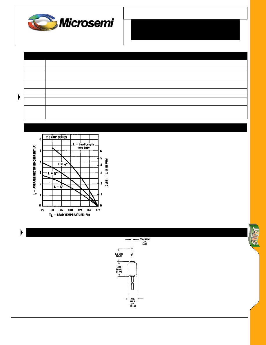
GRAPHS
FIGURE 1
OUTPUT CURRENT vs. LEAD TEMP.
PACKAGE DIMENSIONS inches/[mm]
NOTE: Lead tolerance = +0.002/-0.003 inches

