1500 WATT UNIDIRECTIONAL
TRANSIENT VOLTAGE SUPPRESSOR
Microsemi
Scottsdale Division
8700 E. Thomas Rd. PO Box 1390, Scottsdale, AZ 85252 USA, (480) 941-6300, Fax: (480) 947-1503
Page 1
Copyright
2002
11-06-2003 REV A
W
W
W
.
Mi
c
r
o
s
e
m
i
.
C
O
M
S C O T T S D A L E D I V I S I O N
1N5629 thru 1N5665A
1
N
5
6
2
9
t
h
r
u
1
N
5
6
6
5
A
5
6
2
9
t
h
r
u
1
N
5
6
6
5
A
DESCRIPTION
APPEARANCE
This popular Transient Voltage Suppressor (TVS) series for 1N5629 thru
1N5665A are JEDEC registered selections for unidirectional devices. All
have the same high Peak Pulse Power rating of 1500 W with extremely fast
response times. They are also available in military qualified selections as
described in the Features section herein. They are most often used for
protecting against transients from inductive switching environments,
induced RF effects, or induced secondary lightning effects as found in
lower surge levels of IEC61000-4-5. They are also very successful in
protecting airborne avionics and electrical systems. Since their response
time is virtually instantaneous, they can also protect from ESD and EFT per
IEC61000-4-2 and IEC61000-4-4.
DO-13
(DO-202AA)
IMPORTANT: For the most current data, consult MICROSEMI's website:
http://www.microsemi.com
FEATURES
APPLICATIONS / BENEFITS
� Unidirectional TVS series for thru-hole mounting
� Suppresses transients up to 1500 watts @ 10/1000 �s
(see Figure 1)
� Clamps transient in less than 100 pico seconds
� Working voltage (V
WM
) range 5 V to 171 V
� Hermetic sealed DO-13 metal package
� JAN/TX/TXV military qualifications also available for
the tighter tolerance "A" suffix devices per MIL-PRF-
19500/500 by adding the JAN, JANTX, or JANTXV
prefix, e.g. JANTXV1N5629A, etc.
� For bidirectional TVS in the same DO-13 package,
see separate data sheet for the 1N6036 � 1N6072A
series (also military qualified)
� Surface mount equivalent packages also available as
SMCJ5.0 - SMCJ170CA or SMCG5.0 � SMCG170CA
in separate data sheet (consult factory for other
surface mount options)
� Plastic axial-leaded equivalents available in the
1N6267 � 1N6303A series in separate data sheet
� Protection from switching transients and induced RF
� ESD & EFT protection per IEC 61000-4-2 and -4-4
� Secondary lightning protection per IEC61000-4-5 with
42 Ohms source impedance:
Class 1: 1N5629 to 1N5665A
Class 2: 1N5629 to 1N5663A
Class 3: 1N5629 to 1N5655A
Class 4: 1N5629 to 1N5648A
� Secondary lightning protection per IEC61000-4-5 with
12 Ohms source impedance:
Class 1 : 1N5629 to 1N5658A
Class 2: 1N5629 to 1N5651A
Class 3: 1N5629 to 1N5643A
Class 4: 1N5629 to 1N5636A
� Secondary lightning protection per IEC61000-4-5 with
2 Ohms source impedance:
Class 2: 1N5629 to 1N5642A
Class 3: 1N5629 to 1N5635A
� Inherently radiation hard per Microsemi MicroNote 050
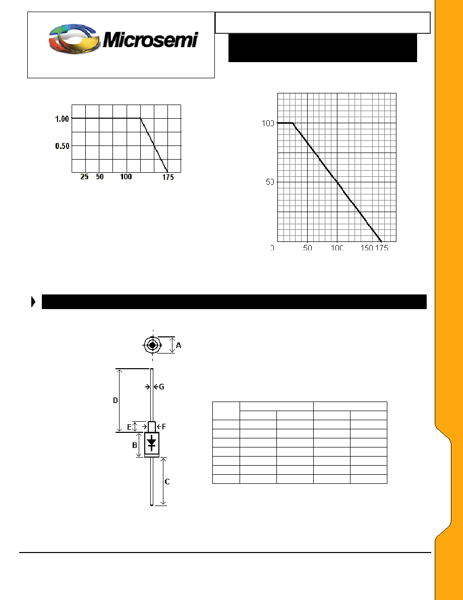
MAXIMUM RATINGS
MECHANICAL AND PACKAGING
� 1500 Watts for 10/1000 �s
with repetition rate of 0.01% or
less*
at lead temperature (T
L
) 25
o
C (See Figs. 1, 2, & 4)
� Operating & Storage Temperatures: -65
o
to +175
o
C
� THERMAL RESISTANCE: 50
o
C/W junction to lead at
0.375 inches (10 mm) from body or 110
o
C/W junction to
ambient when mounted on FR4 PC board with 4 mm
2
copper pads (1 oz) and track width 1 mm, length 25 mm
� DC Power Dissipation
*
: 1 Watt at T
L
< +125
o
C 3/8" (10
mm) from body (see derating in Fig 3 and note below)
� Forward surge current: 200 Amps for 8.3ms half-sine
wave at T
A
= +25
o
C
� Solder Temperatures: 260
o
C for 10 s (maximum)
� CASE: DO-13 (DO-202AA), welded, hermetically
sealed metal and glass
� FINISH: All external metal surfaces are Tin-Lead
plated and solderable per MIL-STD-750 method
2026
� POLARITY: Cathode connected to case and polarity
indicated by diode symbol
� MARKING: Part number and polarity diode symbol
� WEIGHT: 1.4 grams. (Approx)
� TAPE & REEL option: Standard per EIA-296 (add
"TR" suffix to part number)
� See package dimension on last page
*
TVS devices are not typically used for dc power dissipation and are instead operated at or less than their rated standoff voltage
(V
WM
) except for transients that briefly drive the device into avalanche breakdown (V
BR
to V
C
region).

1500 WATT UNIDIRECTIONAL
TRANSIENT VOLTAGE SUPPRESSOR
Microsemi
Scottsdale Division
8700 E. Thomas Rd. PO Box 1390, Scottsdale, AZ 85252 USA, (480) 941-6300, Fax: (480) 947-1503
Page 2
Copyright
2002
11-06-2003 REV A
W
W
W
.
Mi
c
r
o
s
e
m
i
.
C
O
M
S C O T T S D A L E D I V I S I O N
1N5629 thru 1N5665A
1
N
5
6
2
9
t
h
r
u
1
N
5
6
6
5
A
ELECTRICAL CHARACTERISTICS @ T
A
= 25
o
C
Breakdown
Voltage
V
(BR)
@ I
(BR)
Min.
Max.
Breakdown
Current
I
(BR)
Rated
Standoff
Voltage
V
WM
Maximum
Standby
Current
I
D
@ V
WM
Maximum
Clamping
Voltage
V
C
@ I
PP
Maximum
Peak
Pulse
Current
I
PP
Maximum
Temperature
Coefficient of V
(BR)
V(BR)
JEDEC
Type
No.*
V V
mA
V
�A
V A %/
o
C
1N5629
1N5629A
1N5630
1N5630A
6.12
6.45
6.75
7.13
7.48
7.14
8.25
7.88
10
10
10
10
5.50
5.80
6.05
6.40
1000
1000
500
500
10.8
10.5
11.7
11.3
139
143
128
132
.057
.057
.061
.061
1N5631
1N5631A
1N5632
1N5632A
7.38
7.79
8.19
8.65
9.02
8.61
10.0
9.55
10
10
1
1
6.63
7.02
7.37
7.78
200
200
50
50
12.5
12.1
13.8
13.4
120
124
109
112
.065
.065
.068
.068
1N5633
1N5633A
1N5634
1N5634A
9.00
9.5
9.9
10.5
11.0
10.5
12.1
11.6
1
1
1
1
8.10
8.55
8.92
9.40
10
10
5
5
15.0
14.5
16.2
15.6
100
103
93
96
.073
.073
.075
.075
1N5635
1N5635A
1N5636
1N5636A
10.8
11.4
11.7
12.4
13.2
12.6
14.3
13.7
1
1
1
1
9.72
10.2
10.5
11.1
5
5
5
5
17.3
16.7
19.0
18.2
87
90
79
82
.078
.078
.081
.081
1N5637
1N5637A
1N5638
1N5638A
13.5
14.3
14.4
15.2
16.5
15.8
17.6
16.8
1
1
1
1
12.1
12.8
12.9
13.6
5
5
5
5
22.0
21.2
23.5
22.5
68
71
64
67
.084
.084
.086
.086
1N5639
1N5639A
1N5640
1N5640A
16.2
17.1
18.0
19.0
19.8
18.9
22.0
21.0
1
1
1
1
14.5
15.3
16.2
17.1
5
5
5
5
26.5
25.2
29.1
27.7
56.5
59.5
51.5
54
.088
.088
.090
.090
1N5641
1N5641A
1N5642
1N5642A
19.8
20.9
21.6
22.8
24.2
23.1
26.4
25.2
1
1
1
1
17.8
18.8
19.4
20.5
5
5
5
5
31.9
30.6
34.7
33.2
47
49
43
45
.092
.092
.094
.094
1N5643
1N5643A
1N5644
1N5644A
24.3
25.7
27.0
28.5
29.7
28.4
33.0
31.5
1
1
1
1
21.8
23.1
24.3
25.6
5
5
5
5
39.1
37.5
43.5
41.4
38.5
40
34.5
36
.096
.096
.097
.097
1N5645
1N5645A
1N5646
1N5646A
29.7
31.4
32.4
34.2
36.3
34.7
39.6
37.8
1
1
1
1
26.8
28.2
29.1
30.8
5
5
5
5
47.7
45.7
52.0
49.9
31.5
33
29
30
.098
.098
.099
.099
1N5647
1N5647A
1N5648
1N5648A
35.1
37.1
38.7
40.9
42.9
41.0
47.3
45.2
1
1
1
1
31.6
33.3
34.8
36.8
5
5
5
5
56.4
53.9
61.9
59.3
26.5
28
24
25.3
.100
.100
.101
.101
1N5649
1N5649A
1N5650
1N5650A
42.3
44.7
45.9
48.5
51.7
49.4
56.1
53.6
1
1
1
1
38.1
40.2
41.3
43.6
5
5
5
5
67.8
64.8
73.5
70.1
22.2
23.2
20.4
21.4
.101
.101
.102
.102
1N5651
1N5651A
1N5652
1N5652A
50.4
53.2
55.8
58.9
61.6
58.8
68.2
65.1
1
1
1
1
45.4
47.8
50.2
53.0
5
5
5
5
80.5
77.0
89.0
85.0
18.6
19.5
16.9
17.7
.103
.103
.104
.104
1N5653
1N5653A
1N5654
1N5654A
61.2
64.6
67.5
71.3
74.8
71.4
82.5
78.8
1
1
1
1
55.1
58.1
60.7
64.1
5
5
5
5
98.0
92.0
108
103
15.3
16.3
13.9
14.6
.104
.104
.105
.105
1N5655
1N5655A
1N5656
1N5656A
73.8
77.9
81.9
86.5
90.2
86.1
100.0
95.5
1
1
1
1
66.4
70.1
73.7
77.8
5
5
5
5
118
113
131
125
12.7
13.3
11.4
12.0
.105
.105
.106
.106
1N5657
1N5657A
1N5658
1N5658A
90
95
99
105
110
105
121
116
1
1
1
1
81.0
85.5
89.2
94.0
5
5
5
5
144
137
158
152
10.4
11.0
9.5
9.9
.106
.106
.107
.107
1N5659
1N5659A
1N5660
1N5660A
108
114
117
124
132
126
143
137
1
1
1
1
97.2
102
105
111
5
5
5
5
173
165
187
179
8.7
9.1
8.0
8.4
.107
.107
.107
.107
1500 WATT UNIDIRECTIONAL
TRANSIENT VOLTAGE SUPPRESSOR
100
10
1.0
0.1Kw
Microsemi
Scottsdale Division
8700 E. Thomas Rd. PO Box 1390, Scottsdale, AZ 85252 USA, (480) 941-6300, Fax: (480) 947-1503
Page 3
Copyright
2002
11-06-2003 REV A
W
W
W
.
Mi
c
r
o
s
e
m
i
.
C
O
M
S C O T T S D A L E D I V I S I O N
1N5629 thru 1N5665A
1
N
5
6
2
9
t
h
r
u
1
N
5
6
6
5
A
5
6
2
9
t
h
r
u
1
N
5
6
6
5
A
Breakdown
Breakdown
Voltage
Voltage
V
(BR)
@ I
(BR)
V
Min.
Max.
Min.
Max.
Breakdown
Current
Breakdown
Current
I
(BR)
I
Rated
Standoff
Voltage
Rated
Standoff
Voltage
V
WM
V
Maximum
Maximum
Standby
Current
Standby
Current
I
D
@ V
WM
I
Maximum
Clamping
Voltage
Maximum
Clamping
Voltage
V
C
@ I
PP
V
Maximum
Peak
Pulse
Current
Maximum
Peak
Pulse
Current
I
PP
I
Maximum
Temperature
Maximum
Temperature
Coefficient of V
(BR)
V(BR)
Coefficient of V
(BR)
@ I
(BR)
(BR)
WM
D
@ V
WM
C
@ I
PP
PP
(BR)
V(BR)
JEDEC
Type
No.*
V V
mA
V
�A
V A %/
o
C
1N5661
1N5661A
1N5662
1N5662A
135
143
144
152
165
158
176
168
1
1
1
1
121
128
130
136
5
5
5
5
215
207
230
219
7.0
7.2
6.5
6.8
.108
.108
.108
.108
1N5663
1N5663A
1N5664
1N5664A
153
162
162
171
187
179
198
189
1
1
1
1
138
145
146
154
5
5
5
5
244
234
258
246
6.2
6.4
5.8
6.1
.108
.108
.108
.108
1N5665
1N5665A
180
190
220
210
1
1
162
171
5
5
287
274
5.2
5.5
.108
.108
* No suffix = 10% tolerance, suffix A = 5% tolerance. Suffix A also available in military qualified types with a JAN, JANTX, or JANTXV prefix.
NOTES: V
(BR)
is measured after I
(BR)
has been applied for < 300ms.
Forward
voltage
V
F
at 100 amps peak 8.3 ms is 3.5 volts max.
SYMBOLS & DEFINITIONS
Symbol Definition
V
WM
Standoff Voltage: Applied Reverse Voltage to assure a nonconductive condition. (See Note 1.)
V
(BR)
Breakdown Voltage: This is the Breakdown Voltage the device will exhibit at 25
o
C
V
C
Maximum Clamping Voltage: The maximum peak voltage appearing across the TVS when subjected to the
peak pulse current in a one millisecond time interval. The peak pulse voltage is the combination of voltage rise
due to both the series resistance and thermal rise and positive temperature coefficient (
V(BR)
)
I
PP
Peak Pulse Current: The peak current during the impulse (See Figure 2)
P
PP
Peak Pulse Power: The pulse power as determined by the product of V
C
and I
PP
I
D
Standby Current: The current at the standoff voltage (V
WM
)
I
(BR)
Breakdown Current: The current used for measuring Breakdown Voltage (V
(BR)
)
NOTE 1: A TVS is normally selected according to the rated "Standoff Voltage" V
WM
that should be equal to or greater than the dc or
continuous peak operating voltage level.
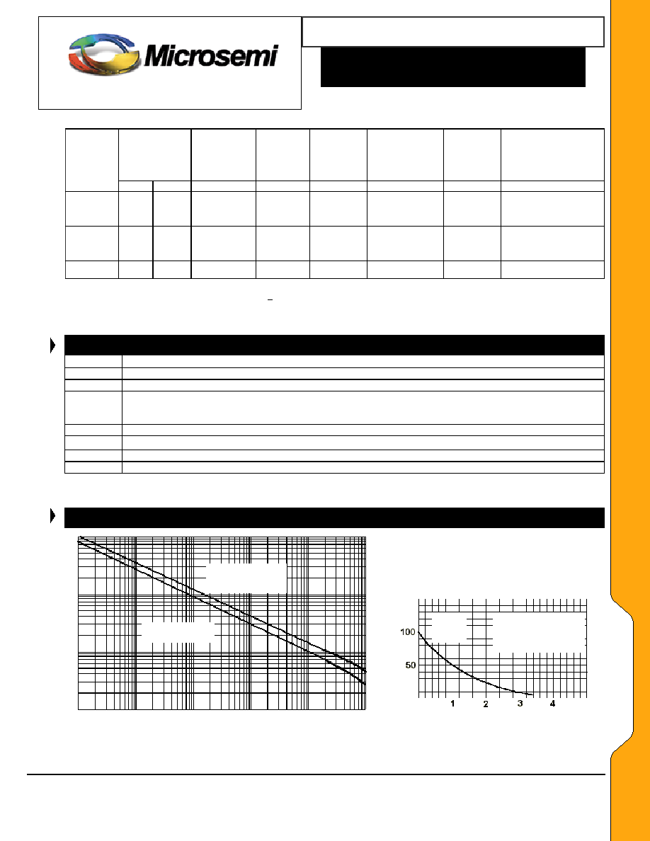
GRAPHS
100ns 1
�s 10�s 100�s 1ms 10ms
Pulse current (I
P
)
in percent of I
PP
Square-wave pulse
Exponential wave-form
(See FIG. 2)
Peak
Pulse
P
ower
(P
PP
)i
n
K
w
Peak Value
I
PP
Pulse time duration (tp) is
defined as that point where
I
P
decays to 50% of peak
value (I
PP
).
time (t) in milliseconds
Pulse Time (tp) FIG.
2 Pulse wave form for exponential surge
FIG. 1 � Non-repetive peak pulse power rating curve
NOTE: Peak power defined as peak voltage times peak current