6.2 & 6.55 Volt Temperature Compensated
Zener Reference Diodes
Microsemi
Scottsdale Division
8700 E. Thomas Rd. PO Box 1390, Scottsdale, AZ 85252 USA, (480) 941-6300, Fax: (480) 947-1503
Page 1
Copyright
2003
10-27-2003 REV C
W
W
W
.
Mi
c
r
o
s
e
m
i
.
C
O
M
S C O T T S D A L E D I V I S I O N
1N821 thru 1N829A-1 DO-7
1
N
8
2
1
--
1
N
8
2
9
A
-
1
DESCRIPTION
APPEARANCE
The popular 1N821 thru 1N829 series of Zero-TC Reference Diodes
provides a selection of both 6.2 V and 6.55 V nominal voltages and
temperature coefficients to as low as 0.0005%/
o
C for minimal voltage
change with temperature when operated at 7.5 mA. These glass axial-
leaded DO-7 reference diodes are also available in JAN, JANTX, JANTXV,
and JANS military qualifications. Microsemi also offers numerous other
Zener Reference Diode products for a variety of other voltages up to 200 V.
IMPORTANT: For the most current data, consult MICROSEMI's website:
http://www.microsemi.com
FEATURES
APPLICATIONS / BENEFITS
∑ JEDEC registered 1N821 thru 1N829 series
∑ Internal metallurgical bonds
∑ Double anode option with 1N822 and 1N824 selection
∑ Reference voltage selection of 6.2 V & 6.55 V +/-5%
with further tight tolerance options at nominal of 6.35 V
∑ 1N821, 823, 825, 827 and 829 also have military
qualification to MIL-PRF-19500/159 up to the JANS
level by adding JAN, JANTX, JANTXV, or JANS
prefixes to part numbers as well as the "-1" suffix, e.g.
JANTX1N829-1, etc.
∑ Radiation Hardened devices available by changing
"1N" prefix to "RH", e.g. RH827, RH 829, RH829A,
etc. Also consult factory for "RH" data sheet brochure
∑ Military surface mount equivalents also available in
DO-213AA with UR-1 suffix and JAN, JANTX, or
JANTXV prefix, e.g. JANTX1N829UR-1 (see separate
data sheet)
∑ Also available in smaller axial-leaded DO-35 package
(see separate data sheet)
∑ Provides minimal voltage changes over a broad
temperature range
∑ For instrumentation and other circuit designs
requiring a stable voltage reference
∑ Maximum temperature coefficient selections
available from 0.01%/∫C to 0.0005%/∫C
∑ Tight voltage tolerances with nominal reference
voltages of 6.35 V available by adding tolerance
1%, 2%, 3%, etc. after the part number for
identification e.g. 1N827-2%, 1N829A -1%, 1N829-
1-1%, etc.
∑ Flexible axial-lead mounting terminals
∑ Nonsensitive to ESD per MIL-STD-750 Method
1020
MAXIMUM RATINGS
MECHANICAL AND PACKAGING
∑ Operating & StorageTemperature: -65
o
C to +175
o
C
∑ DC Power Dissipation: 500 mW @ T
L
= 25
o
C and
maximum current I
ZM
of 70 mA. NOTE: For optimum
voltage-temperature stability, I
Z
= 7.5 mA (less than 50
mW in dissipated power)
∑ Solder temperatures: 260
o
C for 10 s (maximum)
∑ CASE: Hermetically sealed glass case with DO-7
(DO-204AA) package
∑ TERMINALS: Tin-lead plated and solderable per
MIL-STD-750, Method 2026
∑ MARKING: Part number and cathode band (except
double anode 1N822 and 1N824)
∑ POLARITY: Reference diode to be operated with
the banded end positive with respect to the
opposite end
∑ TAPE & REEL option: Standard per EIA-296 (add
"TR" suffix to part number)
∑ WEIGHT: 0.2 grams.
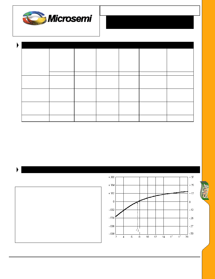
∑ See package dimensions on last page
DO-7
(DO-204AA)
6.2 & 6.55 Volt Temperature Compensated
Zener Reference Diodes
S C O T T S D A L E D I V I S I O N
1N821 thru 1N829A-1 DO-7
W
W
W
.
Mi
c
r
o
s
e
m
i
.
C
O
M
1
N
8
2
1
--
1
N
8
2
9
A
-
1
*ELECTRICAL CHARACTERISTICS @ 25
o
C, unless otherwise specified
ZENER
VOLTAGE
(Note 1 and 4)
V
Z
@ I
ZT
ZENER
TEST
CURRENT
I
ZT
MAXIMUM
ZENER
IMPEDANCE
(Note 2)
Z
ZT
@ I
ZT
MAXIMUM
REVERSE
CURRENT
I
R
@ 3 V
VOLTAGE
TEMPERATURE
STABILITY
(
V
ZT
MAX)
-55
o
C to +100
o
C
(Note 3 and 4)
EFFECTIVE
TEMPERATURE
COEFFICIENT
VZ
JEDEC
TYPE NUMBER
(Note 1, 5 & 6)
VOLTS mA OHMS µA
mV
%/
o
C
1N821
1N821A
1N822
1N823
5.9 ≠ 6.5
5.9 ≠ 6.5
5.9 ≠ 6.5
5.9 ≠ 6.5
7.5
7.5
7.5
7.5
15
10
15
15
2.0
2.0
2.0
2.0
96
96
96
48
0.01
0.01
0.01
0.005
1N823A
1N824
1N825
1N825A
5.9 ≠ 6.5
5.9 ≠ 6.5
5.9 ≠ 6.5
5.9 ≠ 6.5
7.5
7.5
7.5
7.5
10
15
15
10
2.0
2.0
2.0
2.0
48
48
19
19
0.005
0.005
0.002
0.002
1N826
1N827
1N827A
1N828
6.2 ≠ 6.9
5.9 ≠ 6.5
5.9 ≠ 6.5
6.2 ≠ 6.9
7.5
7.5
7.5
7.5
15
15
10
15
2.0
2.0
2.0
2.0
20
9
9
10
0.002
0.001
0.001
0.001
1N829
1N829A
5.9 ≠ 6.5
5.9 ≠ 6.5
7.5
7.5
15
10
2.0
2.0
5
5
0.0005
0.0005
*JEDEC Registered Data.
Double Anode; electrical specifications apply under both bias polarities.
NOTES:
1.
Add a "-1" suffix for internal metallurgical bond. When ordering devices with tighter tolerances than specified for the V
Z
voltage nominal of
6.35 V, add a hyphened suffix to the part number for desired tolerance, e.g. 1N827-1-2%, 1N829-1-1%, 1N829A-1%, 1N829A-1-1%, etc.
2.
Zener impedance measured by superimposing 0.75 mA ac rms on 7.5 mA dc @ 25
o
C.
3.
The maximum allowable change observed over the entire temperature range i.e., the diode voltage will not exceed the specified mV
change at discrete temperature between the established limits.
4.
Voltage measurements to be performed 15 seconds after application of dc current.
5.
1N821, 1N823, 1N825, 1N827, and 1N829 also have qualification to MIL-PRF-19500/159 by adding the JAN,
JANTX, JANTXV, or
JANS prefix to part numbers as well as the "-1" suffix; e.g. JANTX1N827-1, JANTXV1N829-1, etc.
6.
Designate Radiation Hardened devices with "RH" prefix instead of "1N", e.g. RH829A instead of 1N829A.
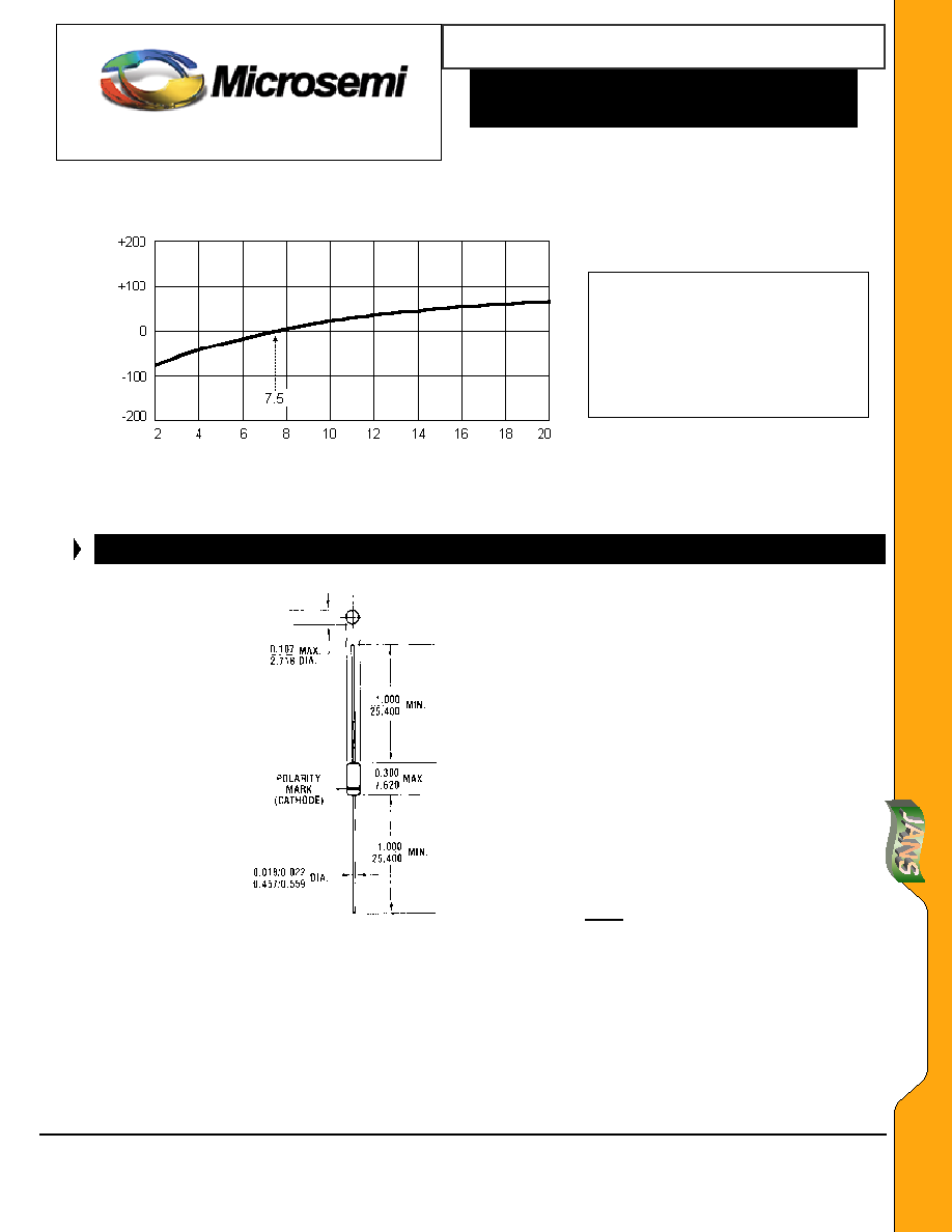
GRAPHS
Change in tempe
r
ature coefficient
(%/
o
C)
Change in tempe
r
ature coefficient
(mV/
o
C)
FIGURE
1
TYPICAL CHANGE OF TEMPERATURE COEFFICIENT
The curve shown in Figure 1 is typical of the diode series and
greatly simplifies the estimation of the Temperature Coefficient
(TC) when the diode is operated at currents other than 7.5mA.
EXAMPLE: A diode in this series is operated at a current of
7.5mA and has specified Temperature Coefficient (TC) limits of
+/-0.005%/
o
C. To obtain the typical Temperature Coefficient
limits for this same diode operated at a current of 6.0mA, the
new TC limits (%/
o
C) can be estimated using the graph in
FIGURE 1.
At a test current of 6.0mA the change in Temperature Coefficient
(TC) is approximately ≠0.0006%.
o
C. The algebraic sum of +/-
0.005%
o
C and ≠0.0006%/
o
C gives the estimated limits of
+0.0044%/
o
C and -0.0056%/
o
C.
WITH CHANGE IN OPERATING CURRENT.
Microsemi
Scottsdale Division
8700 E. Thomas Rd. PO Box 1390, Scottsdale, AZ 85252 USA, (480) 941-6300, Fax: (480) 947-1503
Page 2
Copyright
2003
10-27-2003 REV C