A
D V A N C E D
P W M C
O N T R O L L E R
P
R O D U C T I O N
D
A T A
S
H E E T
T
H E
I
N F I N I T E
P
O W E R
O F
I
N N O V A T I O N
LX1660/1661
LIN D
O C
#: 1660
D E S C R I P T I O N
K E Y F E A T U R E S
s Designed To Drive A Synchronous Rectifier
Stage -- Can Also Be Used In Non-
Synchronous Applications
s Soft-Start Capability
s Hiccup-Mode Fault Protection
s No Current-Sense Resistor Required For
Current Limiting
s Modulated Constant Off-Time Control
Mechanism For Fast Transient Response And
Simple System Design
s 2V, 0.5% Internal Voltage Reference Brought
Out
The LX1660 and LX1661 Are Mono-
lithic Switching Regulator Controller
ICs designed to provide low-cost, high-
performance adjustable power supply for
microprocessors and other applications
requiring a fast transient response and a
high degree of accuracy. They provide
an adjustable synchronous Pulse Width
Modulator output suitable for a power
supply for Pentium
�
or other micropro-
cessors.
Synchronous Rectifier Driver For
CPU Core. The devices can drive dual
MOSFETs resulting in typical efficiencies
of 85 - 90%, even with loads in excess of
10A. Synchronous shutdown results in
increased efficiency in light load applica-
tions.
Short-Cir cuit Current Limiting
Without Expensive Current Sense Re-
sistors. The current sensing mechanism
can use a PCB trace resistance or the para-
sitic resistance of the main inductor. For
applications requiring a high degree of
accuracy, a conventional sense resistor
can be used.
Hiccup Mode Fault Protection. The
hiccup mode is programmable and with
pulse-by-pulse current limiting will help
protect the power supply system and load
in the even of a short circuit.
Ultra-Fast Transient Response Re-
duces System Cost. The fixed frequency
modulated off-time architecture results in
the fastest transient response for a given
inductor. Adaptive voltage positioning
(LX1661 only) requires fewer low-ESR ca-
pacitors to meet stringent transient over-
and under-shoot specifications.
P R O D U C T H I G H L I G H T
P A C K A G E O R D E R I N F O R M A T I O N
T
A
(�C)
Plastic DIP
16-pin
0 to 70
LX166xCN
LX166xCD
N
Plastic SOIC
16-pin
D
LX1661 I
N
S
OCKET
7
P
ROCESSOR
S
UPPLY
A
PPLICATION
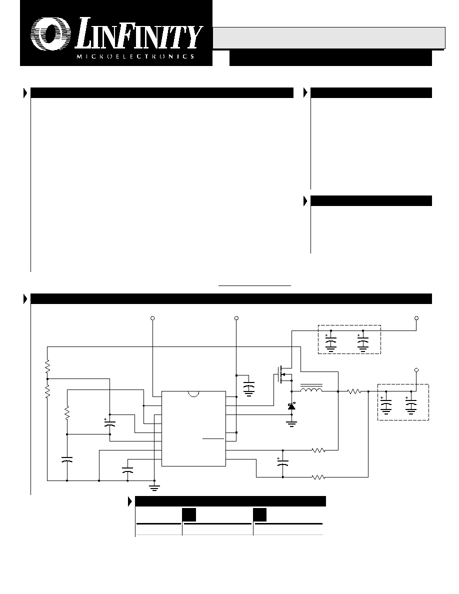
A P P L I C A T I O N S
s Pentium Processor Supplies
s AMD-K6
TM
Supplies
s Cyrix
�
6x86
TM
Supplies
s Voltage Regulator Modules
s General Purpose DC:DC Supplies
Note: All surface-mount packages are available in Tape & Reel.
Append the letter "T" to part number. (i.e. LX166xCDT)
EN
C
T
C8
390pF
TDRV
V
CC
CS-
OT
ADJ
SGND
V
REF
INV
NINV
HICCUP
CS+
SYNCEN
BDRV
PGND
V
C1
LX1661
R16
10k
C3
0.1�F
C4
390pF
R15
2.0k
1%
R14, 1%
See Table 5
C9
1�F
12V
L1
R1, 5m
16V, 1000�F
Sanyo MV-GX or
equivalent
V
OUT
16V, 1000�F
Sanyo MV-GX or equivalent
V
IN
5V
16-pin SOIC
C1
390pF
Q1
IRL3103
5�H Toroid
D1
C5
16
15
14
13
12
11
10
9
1
2
3
4
5
6
7
8
C2
C7
C6
OUTEN
U1
R5, 1k
R6, 1k
Copyright � 1998
Rev. 1.1 7/98
1
11861 W
ESTERN
A
VENUE
, G
ARDEN
G
ROVE
, CA. 92841, 714-898-8121, F
AX
: 714-893-2570
L
I N
F
I N I T Y
M
I C R O E L E C T R O N I C S
I
N C
.
IMPORTANT: For the most current data, consult LinFinity's web site: http://www.linfinity.com.

A
D V A N C E D
P W M C
O N T R O L L E R
LX1660/1661
P R O D U C T D A T A B O O K 1 9 9 6 / 1 9 9 7
Copyright � 1998
Rev. 1.1 7/98
2
P
R O D U C T I O N
D
A T A
S
H E E T
ABSOLUTE MAXIMUM RATINGS
(Note 1)
Supply Voltage ............................................................................................................. 25V
Output Peak Current Source (500ns) ......................................................................... 1.5A
Output Peak Current Sink (500ns) ............................................................................. 1.5A
Analog Inputs ................................................................................................... -0.3 to +6V
Power Dissipation at T
A
= 25�C
N Package ............................................................................................................... 1.5W
D Package ........................................................................................................... 830mW
Operating Junction Temperature
Plastic (N, D Packages) ......................................................................................... 150�C
Storage Temperature Range .................................................................... -65�C to +150�C
Lead Temperature (Soldering, 10 Seconds) ............................................................. 300�C
PACKAGE PIN OUTS
1
16
2
15
3
14
4
13
5
12
6
11
7
10
8
9
D PACKAGE
(Top View)
N PACKAGE:
THERMAL RESISTANCE-JUNCTION TO AMBIENT,
JA
65�C/W
D PACKAGE:
THERMAL RESISTANCE-JUNCTION TO AMBIENT,
JA
120�C/W
Junction Temperature Calculation: T
J
= T
A
+ (P
D
x
JA
).
The
JA
numbers are guidelines for the thermal performance of the device/pc-board system.
All of the above assume no ambient airflow
THERMAL DATA
Note 1. Exceeding these ratings could cause damage to the device. All voltages are with respect
to Ground. Currents are positive into, negative out of the specified terminal. Pin
numbers refer to DIL packages only.
V
C1
TDRV
PGND
BDRV
V
CC
SYNCEN
CS+
CS-
EN
OT
ADJ
SGND
V
REF
INV
NINV/SS
HICCUP
C
T
1
16
2
15
3
14
4
13
5
12
6
11
7
10
8
9
N PACKAGE
(Top View)
V
C1
TDRV
PGND
BDRV
V
CC
SYNCEN
CS+
CS-
EN
OT
ADJ
SGND
V
REF
INV
NINV/SS
HICCUP
C
T
A
D V A N C E D
P W M C
O N T R O L L E R
LX1660/1661
P R O D U C T D A T A B O O K 1 9 9 6 / 1 9 9 7
3
Copyright � 1998
Rev. 1.1 7/98
P
R O D U C T I O N
D
A T A
S
H E E T
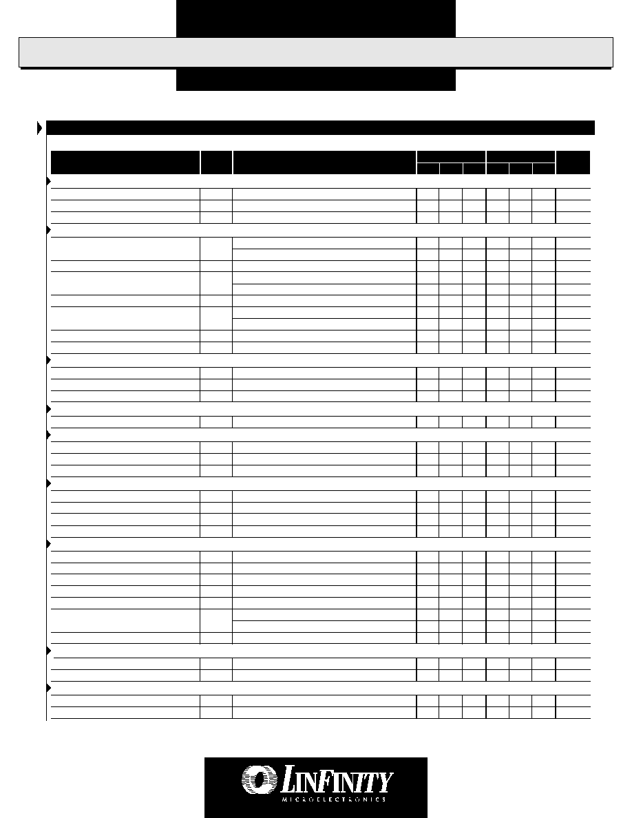
E L E C T R I C A L C H A R A C T E R I S T I C S
(Unless otherwise specified, 10.8 < V
CC
< 13.2, 0�C
T
A
85�C. Test conditions: V
CC
= 12V, T = 25�C.)
Reference Section
Parameter
Symbol
Test Conditions
Initial Output Voltage
V
CC
= 12V, I
L
= 100�A
Load Regulation
V
CC
= 12V, I
L
= 10�A to 5mA
Short Circuit Current I
SH
V
REF
= 1.96V
LX1661
Units
Min. Typ. Max. Min. Typ. Max.
LX1660
1.98
2
2.02 1.98
2
2.02
V
2
2
mV
24
24
mA
Timing Section
Off Time Initial
OT
OT
ADJ
= 1.8V, C
T
= 390pF
OT
ADJ
= 3.5V, C
T
= 390pF
Off Time Temp Stability
OT
ADJ
= 1.8V to 3.5V
Discharging Current
I
DIS
V
NINV
= 1.8V, V
CT
= 1.5V
V
NINV
= 3.5V, V
CT
= 1.75V
Ramp Peak
V
P
Ramp Peak-Valley
V
RPP
OT
ADJ
= 1.8V
OT
ADJ
= 3.5V
Ramp Valley Delay to Output
10% Overdrive
Turn Off Threshold
V
OFF
(Voltage at OT
ADJ
Pin)
2
2
�S
1
1
�S
2
2
%
180
210
240
180
210
240
�A
180
210
240
180
210
240
�A
2
2
V
0.8
0.9
1.0
0.8
0.9
1.0
V
0.475 0.5 0.525 0.475 0.5 0.525
V
100
100
nS
0.6
0.9
1.2
0.6
0.9
1.2
V
Input Bias Current
I
B
1.8V < V
CS
+ = V
CS
< 3.5V
Pulse By Pulse C
L
V
CLP
Initial Accuracy
C
S
Delay to Output
10% Overdrive
Error Comparator Section
Synchronous Control Section
Synchronous Enable Threshold
S
YCEN
Current Sense Section
0.1
1.0
0.1
1.0
�A
2
36
42
48
mV
150
150
nS
0.5
0.7
0.9
0.5
0.7
0.9
V
0.1
1
0.1
1
�A
80
90
100
80
90
100
mV
150
150
nS
Input Bias Current
I
B
V
FB
= V
SET
Input Offset Voltage
V
IO
E
C
Delay to Output
10% Overdrive
Output Drivers Section
Output Rise Time
T
R
V
CL
= V
C2
= 12V, C
L
= 3000pF
Output Fall Time
T
F
V
CL
= V
C2
= 12V, C
L
= 3000pF
Output Pull Down
V
PD
V
CC
= V
C
= 0, I
PULL UP
= 2mA
Peak Current
I
PK
t
PULSE
= 500ns
70
70
nSec
70
70
nSec
1
1
V
1.0
1.0
A
UVLO and S.S. Section
Start-Up Threshold
V
ST
Hysteresis
V
HYST
S.S. Sink Current
I
SD
V
CL
= 10.1V
S.S. Sat Voltage
V
OL
V
CL
= 9V, I
SD
= 20�A
Enable Shutdown Threshold
V
EN
Enable Bias Current
I
EN
I
EN
(Low), V
EN
= 0V
I
EN
(High), V
EN
= 2V
Enable Hysteresis
9.85 10.15 10.45 9.85 10.15 10.45
V
0.31
0.31
V
2
3
2
3
mA
0.2
0.6
0.2
0.6
V
1.3
1.4
1.5
1.3
1.4
1.5
V
-0.5
-1
-0.5
-1
�A
0.5
1
0.5
1
�A
0.14 0.16 0.18 0.14 0.16 0.18
V
Supply Current Section
Dynamic Operating Current
I
CD
V
CC
= V
C
= 12V, Out Freq = 200kHz, C
L
= 0
Start-Up Current
I
ST
V
CL
= 10V
25
25
mA
500 1000
500 1000
�A
Hiccup Section
Hiccup Factor "ON" Time
(C
HICCUP
= 0.1�F typ.)
Hiccup Duty Cycle
100
100
mS/�F
10
10
%

A
D V A N C E D
P W M C
O N T R O L L E R
LX1660/1661
P R O D U C T D A T A B O O K 1 9 9 6 / 1 9 9 7
Copyright � 1998
Rev. 1.1 7/98
4
P
R O D U C T I O N
D
A T A
S
H E E T
B L O C K D I A G R A M
1
EN
INTERNAL
V
CC
2
OT
ADJ
2V REF
EN
UVLO
10.6/10.1
2V OUT
V
CC
1.4V
VREG 5V
3
SGND
4
V
REF
5
INV
6
NINV/SS
7
HICCUP
OFFTIME CONTROL
8
C
T
S
R
Q
Q
R DOM
BREAK
BEFORE
MAKE
16
V
C1
15
TDRV
14
PGND
12
V
CC
11
SYNCEN
10
CS+
9
CS-
SYNC EN
COMP
I
MAX
PWM LATCH
ENABLE
ERROR
COMP
O
TADJ
V
PEAK
= 2V
V
VAL
= 1V
S
R
Q
Q
V
CC
HICCUP
90mV
10
I
I
UPGRADE
VREG GOOD
0.7V
HICCUP LATCH
13
BDRV
40mV (1661 only)
1.5V
FIGURE 1 -- Block Diagram

A
D V A N C E D
P W M C
O N T R O L L E R
LX1660/1661
P R O D U C T D A T A B O O K 1 9 9 6 / 1 9 9 7
5
Copyright � 1998
Rev. 1.1 7/98
P
R O D U C T I O N
D
A T A
S
H E E T
EN
1
A low voltage at this pin puts the IC in sleep-mode.
OT
ADJ
2
The purpose of this pin is to allow modulation of the OFF-time relative to the reference voltage. The OFF-time is
inversely proportional to the reference voltage. The inverting input of the upgrade voltage comparator is also
connected to this pin, when the voltage at this pin is below 0.7V, the controller shuts down.
SGND
3
This pin is the signal ground of the IC.
V
REF
4
2V reference.
INV
5
This pin is the inverting input of the error comparator.
NINV/SS
6
This pin is the non-inverting input of the error comparator (LX1661 only: 40mV offset between this pin and error
comparator). This pin is pulled low during sleep-mode to allow soft-start function during start up.
HICCUP
7
A hiccup-mode capacitor connected to this pin adjusts duty cycle.
C
T
8
The OFF-time is programmed by connecting a capacitor from this pin to ground.
CS-
9
This is the inverting input of the pulse-by-pulse current comparator.
CS+
10
This is the non-inverting input of the pulse-by-pulse current comparator.
SYNCEN
11
This pin enables the synchronous (bottom) driver. A high voltage at this pin disables the synchronous driver.
V
CC
12
This is the IC supply voltage as well as the supply to the bottom MOSFET.
BDRV
13
This is the gate drive to the bottom MOSFET
PGND
14
This is a separate ground for the top and bottom MOSFET.
TDRV
15
This is the gate drive to the top MOSFET.
V
C1
16
This pin is a separate power supply input for the top drive.
Pin
#
Description
F U N C T I O N A L P I N D E S C R I P T I O N