 | –≠–ª–µ–∫—Ç—Ä–æ–Ω–Ω—ã–π –∫–æ–º–ø–æ–Ω–µ–Ω—Ç: LX1662ACD | –°–∫–∞—á–∞—Ç—å:  PDF PDF  ZIP ZIP |
D E S C R I P T I O N
K E Y F E AT U R E S
The LX1662/62A and LX1663/63A are
Monolithic Switching Regulator Con-
troller IC's designed to provide a low cost,
high performance adjustable power supply
for advanced microprocessors and other
applications requiring a very fast transient
response and a high degree of accuracy.
Short-Circuit Current Limiting with-
out Expensive Current Sense Resistors.
Current-sensing mechanism can use PCB
trace resistance or the parasitic resistance of
the main inductor. The LX1662A and
LX1663A have reduced current sense com-
parator threshold for optimum perfor-
mance using a PCB trace. For applications
requiring a high degree of accuracy, a
conventional sense resistor can be used to
sense current.
Programmable Synchronous Recti-
fier Driver for CPU Core. The main
output is adjustable from 1.3V to 3.5V using
a 5-bit code. The IC can read a VID signal
set by a DIP switch on the motherboard, or
hardwired into the processor's package (as
in the case of Pentium
Æ
Pro and Pentium II
processors). The 5-bit code adjusts the
output voltage between 1.30 and 2.05V in
50mV increments and between 2.0 and 3.5V
in 100mV increments, conforming to the
I 5-bit Programmable Output For CPU Core
Supply
I No Sense Resistor Required For Short-
Circuit Current Limiting
I Designed To Drive Either Synchronous Or
Non-Synchronous Output Stages
I Lowest System Cost Possible For Price-
Sensitive Pentium And Pentium II Class
Applications
I Soft-Start Capability
I Modulated, Constant Off-Time Architecture
For Fast Transient Response And Simple
System Design
I Available Over-Voltage Protection (OVP)
Crowbar Driver And Power Good Flag
(LX1663 only)
I Small, Surface-Mount Packages
Intel Corporation specification. The device
can drive dual MOSFET's resulting in typical
efficiencies of 85 - 90% even with loads in
excess of 10 amperes. For cost sensitive
applications, the bottom MOSFET can be
replaced with a Schottky diode (non-syn-
chronous operation).
Smallest Package Size. The LX1662 is
available in a narrow body 14-pin surface
mount IC package for space sensitive appli-
cations. The LX1663 provides the additional
functions of Over Voltage Protection (OVP)
and Power Good (PWRGD) output drives
for applications requiring output voltage
monitoring and protection functions.
Ultra-Fast Transient Response Re-
duces System Cost. The modulated off-
time architecture results in the fastest tran-
sient response for a given inductor, reduc-
ing output capacitor requirements, and re-
ducing the total regulator system cost.
Over-Voltage Protection and Power
Good Flag. The OVP output in the LX1663
& LX1663A can be used to drive an SCR
crowbar circuit to protect the load in the
event of a short-circuit of the main MOSFET.
The LX1663 & LX1663A also have a logic-
level Power Good Flag to signal when the
output voltage is out of specified limits.
P R O D U C T H I G H L I G H T
S
INGLE
-C
HIP
P
ROGRAMMABLE
PWM C
ONTROLLERS
WITH
5-B
IT
DAC
P
R O D U C T I O N
D
A T A
S
H E E T
T
H E
I
N F I N I T E
P
O W E R
O F
I
N N O V A T I O N
LX1662/62A, LX1663/63A
LIN D
OC
#: 1662
A P P L I C AT I O N S
I Socket 7 Microprocessor Supplies
(including Intel Pentium Processor, AMD-
K6
TM
And Cyrix
Æ
6x86
TM
, Gx86
TM
and M2
TM
Processors)
I Pentium II and Deschutes Processor & L2-
Cache Supplies
I Voltage Regulator Modules
I General Purpose DC:DC Converter
Applications
P A C K A G E O R D E R I N F O R M AT I O N
T
A
(∞C)
Plastic DIP
14-pin
0 to 70
LX1662CN
LX1663CN
LX1662CD
LX1663CD
LX1662ACN
LX1663ACN
LX1662ACD
LX1663ACD
N
Note: All surface-mount packages are available in Tape & Reel. Append the letter "T" to part number. (i.e. LX1662CDT)
Plastic DIP
16-pin
N
Plastic SOIC
14-pin
D
Plastic SOIC
16-pin
D
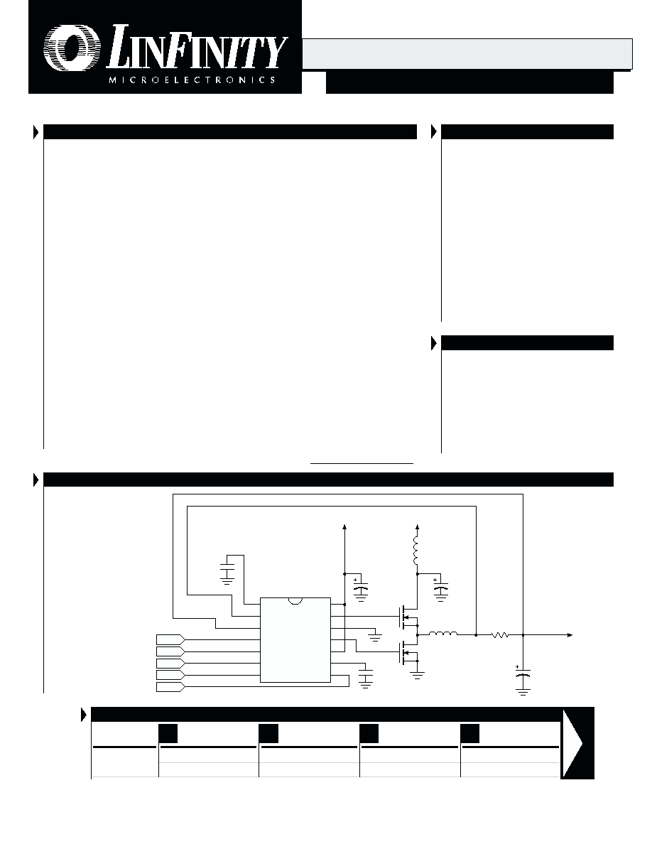
LX1662
IN
A
P
ENTIUM
/P
ENTIUM
II
S
INGLE
-C
HIP
P
OWER
S
UPPLY
S
OLUTION
Copyright © 1999
Rev. 1.1 11/99
1
11861 W
ESTERN
A
VENUE
, G
ARDEN
G
ROVE
, CA. 92841, 714-898-8121, F
AX
: 714-893-2570
L
I N
F
I N I T Y
M
I C R O E L E C T R O N I C S
I
N C
.
IMPORTANT: For the most current data, consult LinFinity's web site: http://www.linfinity.com.
SS
TDRV
V
CC
INV
V
CC_CORE
VID0
VID1
VID2
VID3
VID4
C
T
BDRV
GND
V
C1
U1
LX1662
VID3
C
5
1µF
12V
R
1
V
OUT
5V
14-pin, Narrow Body SOIC
Q
1
IRL3102
L
1
, 2.5µH
6.3V, 1500µF x 3**
14
13
12
11
10
9
1
2
3
4
5
6
7
8
C
8
680pF
VID2
VID1
VID0
VID4
C
3
0.1µF
2.5m
9
Supply Voltage
for CPU Core
6.3V
1500µF x3
** Three capacitors for Pentium
Four capacitors for Pentium II
Q
2
IRL3303
C
1
C
2
L
2
1µH
See next page
for
Selection
Guide
S
INGLE
-C
HIP
P
ROGRAMMABLE
PWM C
ONTROLLERS
WITH
5-B
IT
DAC
LX1662/62A, LX1663/63A
P R O D U C T D A T A B O O K 1 9 9 6 / 1 9 9 7
Copyright © 1999
Rev. 1.1 11/99
2
P
R O D U C T I O N
D
A T A
S
H E E T
ABSOLUTE MAXIMUM RATINGS
(Note 1)
Supply Voltage (V
C1
) .................................................................................................... 25V
Supply Voltage (V
CC
) .................................................................................................... 15V
Output Drive Peak Current Source (500ns) ............................................................... 1.5A
Output Drive Peak Current Sink (500ns) ................................................................... 1.5A
Input Voltage (SS, INV, V
CC_CORE
, C
T
, VID0-VID4) ........................................... -0.3V to 6V
Operating Junction Temperature
Plastic (N & D Packages) ...................................................................................... 150∞C
Storage Temperature Range .................................................................... -65∞C to +150∞C
Lead Temperature (Soldering, 10 Seconds) ............................................................. 300∞C
PACKAGE PIN OUTS
V
C1
TDRV
GND
BDRV
V
CC
C
T
VID4
SS
INV
V
CC_CORE
VID0
VID1
VID2
VID3
1
14
2
13
3
12
4
11
5
10
6
9
7
8
N PACKAGE -- 14-Pin
LX1662/1662A (Top View)
N PACKAGE:
THERMAL RESISTANCE-JUNCTION TO AMBIENT,
JA
65∞C/W
D PACKAGE:
THERMAL RESISTANCE-JUNCTION TO AMBIENT,
JA
120∞C/W
Junction Temperature Calculation: T
J
= T
A
+ (P
D
x
JA
).
The
JA
numbers are guidelines for the thermal performance of the device/pc-board system.
All of the above assume no ambient airflow
THERMAL DATA
Note 1. Exceeding these ratings could cause damage to the device. All voltages are with respect
to Ground. Currents are positive into, negative out of the specified terminal. Pin
numbers refer to DIL packages only.
V
C1
TDRV
GND
BDRV
V
CC
C
T
VID4
SS
INV
V
CC_CORE
VID0
VID1
VID2
VID3
1
14
2
13
3
12
4
11
5
10
6
9
7
8
D PACKAGE -- 14-Pin
LX1662/1662A (Top View)
V
C1
TDRV
GND
BDRV
V
CC
C
T
OV
PWRGD
SS
INV
V
CC_CORE
VID0
VID1
VID2
VID3
VID4
1
16
2
15
3
14
4
13
5
12
6
11
7
10
8
9
N PACKAGE -- 16-Pin
LX1663/1663A (Top View)
V
C1
TDRV
GND
BDRV
V
CC
C
T
OV
PWRGD
SS
INV
V
CC_CORE
VID0
VID1
VID2
VID3
VID4
1
16
2
15
3
14
4
13
5
12
6
11
7
10
8
9
D PACKAGE -- 16-Pin
LX1663/1663A (Top View)
D E V I C E S E L E C T I O N G U I D E
OVP and
Current-Sense
DEVICE
Packages
Power Good
Comp. Thresh. (mV) Optimal Load
LX1662
14-pin SOIC
No
100
Pentium-class (<10A)
LX1662A
& DIP
60
Pentium II (> 10A)
LX1663
16-pin SOIC
Yes
100
Pentium-class (<10A)
LX1663A
& DIP
60
Pentium II (> 10A)
S
INGLE
-C
HIP
P
ROGRAMMABLE
PWM C
ONTROLLERS
WITH
5-B
IT
DAC
LX1662/62A, LX1663/63A
P R O D U C T D A T A B O O K 1 9 9 6 / 1 9 9 7
3
Copyright © 1999
Rev. 1.1 11/99
P
R O D U C T I O N
D
A T A
S
H E E T
E L E C T R I C A L C H A R A C T E R I S T I C S
(Unless otherwise specified, 10.8 < V
CC
< 13.2, 0∞C
T
A
70∞C. Test conditions: V
CC
= 12V, T = 25∞C. Use Application Circuit.)
Reference & DAC Section
(See Table 1 - Next Page)
Parameter
Symbol
Test Conditions
Regulation Accuracy
(See Table 1)
(Less 40mV output adaptive positioning)
, V
CC
= 12V, I
LOAD
= 6A
Regulation Accuracy
1.8V
V
OUT
2.8V
Timing Section
Off Time Initial
OT
V
CC_CORE
= 1.3V, C
T
= 390pF
V
CC_CORE
= 3.5V, C
T
= 390pF
Off Time Temp Stability
V
CC_CORE
= 1.3V to 3.5V
Discharging Current
I
DIS
V
CC_CORE
= 1.3V, V
CT
= 1.5V
Ramp Peak
V
P
Ramp Peak-Valley
V
RPP
V
CC_CORE
= 1.3V
V
CC_CORE
= 3.5V
Ramp Valley Delay to Output
10% Overdrive
Input Bias Current (V
CC_CORE
Pin)
I
B
1.3V < V
INV
= V
CC_CORE
< 3.5V
Pulse By Pulse C
L
LX1662/1663
V
CLP
Initial Accuracy
LX1662A/1663A
Initial Accuracy
C
S
Delay to Output
10% Overdrive
Error Comparator Section
Input Bias Current
I
B
1.3V < V
SS
= V
INV
< 3.5V
Input Offset Voltage
V
IO
E
C
Delay to Output
10% Overdrive
Output Drivers Section
Drive Rise Time
T
R
V
C1
= V
CC
= 12V, C
L
= 3000pF
Drive Fall Time
T
F
V
C1
= V
CC
= 12V, C
L
= 3000pF
Drive High
V
DH
V
CC
= V
CC
= 12V, I
SOURCE
= 20mA
V
CC
= V
CC
= 12V, I
SINK
= 200mA
Drive Low
V
DL
V
CC
= V
CC
= 12V, I
SOURCE
= 20mA
V
CC
= V
CC
= 12V, I
SINK
= 200mA
Output Pull Down
V
PD
V
CC
= V
C
= 0, I
PULL UP
= 2mA
UVLO and S.S. Section
Start-Up Threshold
V
ST
Hysteresis
V
HYST
SS Sink Current
I
SD
V
C1
= 10.1V
SS Sat Voltage
V
OL
V
C1
= 9V, I
SD
= 200µA
Supply Current Section
Dynamic Operating Current
I
CD
V
CC
= V
C1
= 12V, Out Freq = 200kHz, C
L
= 0
Power Good / Over-Voltage Protection Section (LX1663 Only)
Lower Threshold
(V
CC_CORE
/ DAC
OUT
)
Hysteresis
Power Good Voltage Low
I
PWRGD
= 5mA
Over-Voltage Threshold
(V
CC_CORE
/ V
DAC
)
OVP Sourcing Current
V
OV
= 5V
Units
-30
30
mV
-1
1
%
LX1662/1663 (A)
Min.
Typ.
Max.
2
µs
1
µs
40
ppm
180
210
240
µA
2
V
0.9
1
1.1
V
0.37
0.42
0.47
V
100
ns
0.8
2
µA
36
41
46
mV
200
ns
27
35
µA
85
100
115
mV
50
60
70
mV
200
ns
70
ns
70
ns
11
V
10
V
0.06
0.1
V
0.8
1.2
V
0.8
1.4
V
9.9
10.1
10.4
V
0.31
V
2
5.5
mA
0.15
0.6
V
27
mA
88
90
92
%
1
%
0.5
0.7
V
110
117
125
%
30
45
mA
Current Sense Section
S
INGLE
-C
HIP
P
ROGRAMMABLE
PWM C
ONTROLLERS
WITH
5-B
IT
DAC
LX1662/62A, LX1663/63A
P R O D U C T D A T A B O O K 1 9 9 6 / 1 9 9 7
Copyright © 1999
Rev. 1.1 11/99
4
P
R O D U C T I O N
D
A T A
S
H E E T
E L E C T R I C A L C H A R A C T E R I S T I C S
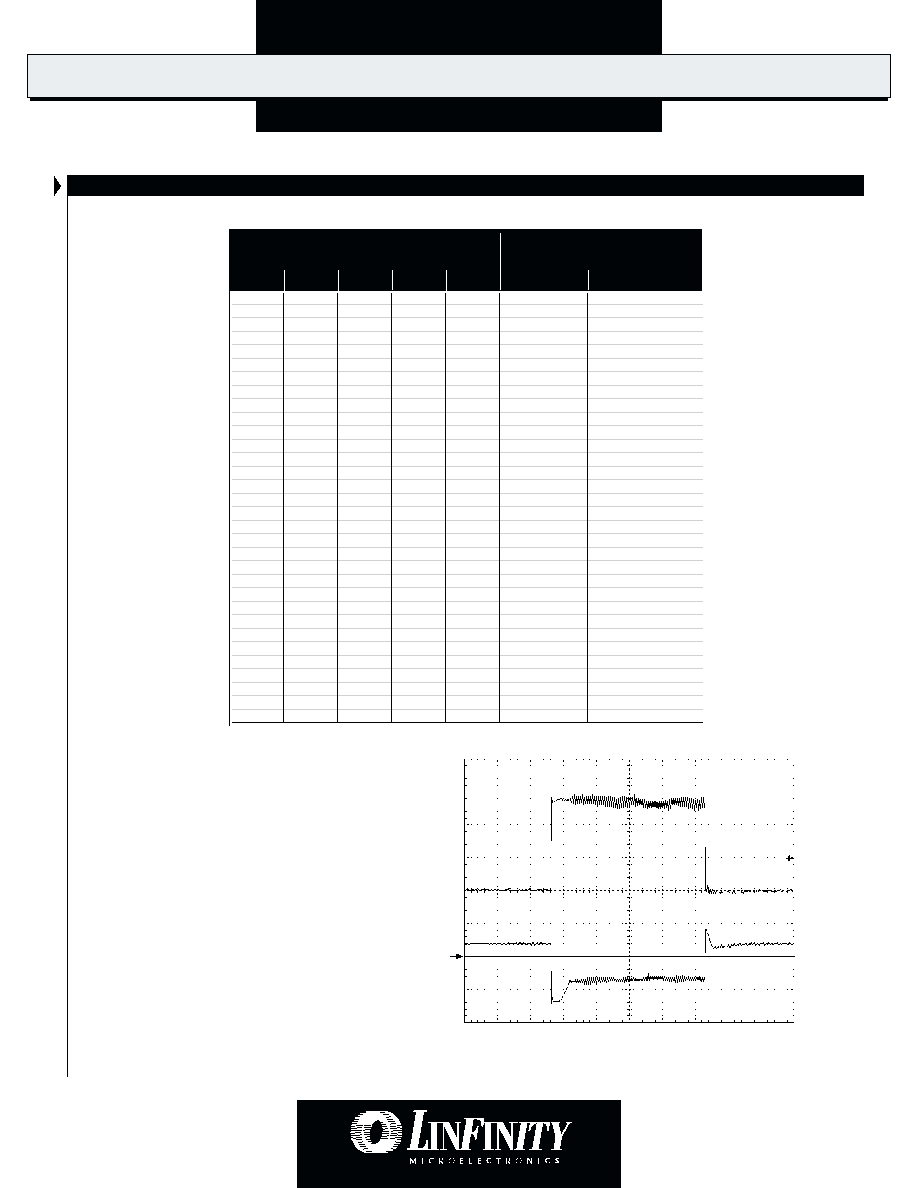
Table 1 - Adaptive Transient Voltage Output
(Output Voltage Setpoint Typical)
0A
5A/Div.
Time - 100µs/Div.
2.8V
100mV/Div.
Output Load
0 to 14A
Output Voltage
FIGURE 1 -- Output Transient Response
(Using 5m
sense resistor and 5µH output inductor)
Note:
Adaptive Transient Voltage Output
In order to improve transient response a
40mV offset is built into the Current Sense
comparator. At high currents, the peak
output voltage will be lower than the
nominal set point , as shown in Figure 1.
The actual output voltage will be a function
of the sense resistor, output current and
output ripple.
0
1
1
1
1
1.34V
1.30V
0
1
1
1
0
1.39V
1.35V
0
1
1
0
1
1.44V
1.40V
0
1
1
0
0
1.49V
1.45V
0
1
0
1
1
1.54V
1.50V
0
1
0
1
0
1.59V
1.55V
0
1
0
0
1
1.64V
1.60V
0
1
0
0
0
1.69V
1.65V
0
0
1
1
1
1.74V
1.70V
0
0
1
1
0
1.79V
1.75V
0
0
1
0
1
1.84V
1.80V
0
0
1
0
0
1.89V
1.85V
0
0
0
1
1
1.94V
1.90V
0
0
0
1
0
1.99V
1.95V
0
0
0
0
1
2.04V
2.00V
0
0
0
0
0
2.09V
2.05V
1
1
1
1
1
2.04V
2.00V
1
1
1
1
0
2.14V
2.10V
1
1
1
0
1
2.24V
2.20V
1
1
1
0
0
2.34V
2.30V
1
1
0
1
1
2.44V
2.40V
1
1
0
1
0
2.54V
2.50V
1
1
0
0
1
2.64V
2.60V
1
1
0
0
0
2.74V
2.70V
1
0
1
1
1
2.84V
2.80V
1
0
1
1
0
2.94V
2.90V
1
0
1
0
1
3.04V
3.00V
1
0
1
0
0
3.14V
3.10V
1
0
0
1
1
3.24V
3.20V
1
0
0
1
0
3.34V
3.30V
1
0
0
0
1
3.44V
3.40V
1
0
0
0
0
3.54V
3.50V
VID4
VID3
VID2
VID1
VID0
Processor Pins
Output Voltage (V
CC_CORE
)
0 = Ground, 1 = Open (Floating)
0.0A
Nominal Output*
* Nominal = DAC setpoint voltage with no adaptive output voltage positioning.
S
INGLE
-C
HIP
P
ROGRAMMABLE
PWM C
ONTROLLERS
WITH
5-B
IT
DAC
LX1662/62A, LX1663/63A
P R O D U C T D A T A B O O K 1 9 9 6 / 1 9 9 7
5
Copyright © 1999
Rev. 1.1 11/99
P
R O D U C T I O N
D
A T A
S
H E E T
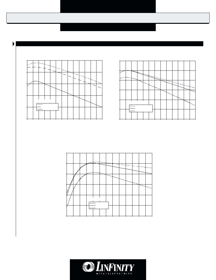
C H A R A C T E R I S T I C S C U R V E S
70
75
80
85
90
95
1
2
3
4
5
6
7
8
9
10
11
12
13
14
I
OUT
(A)
EFFICIENCY (%)
__
EFFICIENCY AT 3.1V
EFFICIENCY AT 2.8V
EFFICIENCY AT 1.8V
Output Set Point
FIGURE 2 -- Efficiency Test Results:
Non-Synchronous Operation, V
IN
= 5V
FIGURE 3 -- Efficiency Test Results:
Synchronous Operation, V
IN
= 5V
FIGURE 4 -- Efficiency Test Results: Synchronous Operation, V
IN
= 12V.
Note: Non-synchronous operation not recommended for 12V operation, due to power loss in Schottky diode.
60
65
70
75
80
85
90
1
2
3
4
5
6
7
8
9
10
11
12
13
14
I
OUT
(A)
1.8V EFFICIENCY
2.8V EFFICIENCY
3.3V EFFICIENCY
Output Set Point
70
75
80
85
90
95
100
1
2
3
4
5
6
7
8
9
10
11
12
13
14
I
OUT
(A)
EFFICIENCY (%)
__
EFFICIENCY AT 3.1V
EFFICIENCY AT 2.8V
EFFICIENCY AT 1.8V
Output Set Point