D E S C R I P T I O N
K E Y F E A T U R E S
s
s
s
s
s Integrated Switching (Class-D) Stereo
Power Amplifier Controller IC
s
s
s
s
s Delivers >10W
RMS
Across 8
/Channel
(20W
RMS
stereo)
s
s
s
s
s Output Power Limited Only By External
FETs And Available Supply Voltage
s
s
s
s
s Will Drive A Wide Range Of Speakers
s
s
s
s
s High Efficiency (>92%)
s
s
s
s
s Due To High Efficiency, Power FETs Do Not
Require Heatsinking
s
s
s
s
s Audio Bandwidth Of 20Hz to 20kHz
s
s
s
s
s Wide Input Voltage Range Of 7V-15V
s
s
s
s
s Low Output Signal Distortion <1%
s
s
s
s
s High Operating Frequency (350kHz) Helps
To Reduce Output Filter Size
s
s
s
s
s Compact Design Minimizes EMI / RFI
The LX1720 is a highly-integrated,
Switching Class-D Stereo Power Am-
plifier Controller IC with power and
size features that make it ideal for multi-
media computer applications, as well as
other applications where high fidelity
sound is required.
With input voltage ranging from 7V-
15V, the LX1720 is designed to operate
over the full 20Hz to 20kHz audio range.
Signal distortion measurements using
industry standard 1kHz signal yields THD
+ noise levels < 1% (10 watts output).
P R O D U C T H I G H L I G H T
S
WITCHING
C
LASS
-D, S
TEREO
P
OWER
A
MPLIFIER
C
ONTROLLER
IC
P
R O D U C T I O N
D
A T A
S
H E E T
T
H E
I
N F I N I T E
P
O W E R
O F
I
N N O V A T I O N
LX1720
Its high efficiency (>92%) eliminates the
need for heat sinks -- even while deliv-
ering more than 10W
RMS
across 8 ohms
per channel (20W
RMS
stereo) with 0.1 ohm
SO-8 power FETs.
The LX1720's output power is limited
only by external FETs and available sup-
ply voltage.
While offering breakthrough perfor-
mance capabilities for notebooks, the
LX1720 is equally attractive for multime-
dia systems or to drive full-size home
theatre speakers.
Copyright � 1999
Rev. 1.0 9/99
1
11861 W
ESTERN
A
VENUE
, G
ARDEN
G
ROVE
, CA. 92841, 714-898-8121, F
AX
: 714-893-2570
L
I N
F
I N I T Y
M
I C R O E L E C T R O N I C S
I
N C
.
APPLICATIONS / BENEFITS
Notebook Computers:
s
s
s
s
s Replaces existing internal low power linear
amplifier with a high efficiency Class-D
amplifier
s
s
s
s
s Enables the use of virtually any external
speaker without amplification
s
s
s
s
s Precious battery life is extended
s
s
s
s
s Fully protected power topology can
withstand shorts or external speaker
failures without damage, overheating or
posing fire hazard
Desktop Computers:
s
s
s
s
s Output power capability of up to 20W
RMS
per channel in an area less than 3"x3",
without using expensive heatsinks
s
s
s
s
s Greatly reduced power supply
requirements when compared to a linear
solution of same power capabilities
s
s
s
s
s Any speakers can be used including
conventional home stereo speakers
s
s
s
s
s Very light weight circuitry will not add to
the overall weight of the system
s
s
s
s
s Multimedia amplifier can be directly
incorporated on the motherboard using
surface mount components
0 to 70
15V
LX1720-01CDB
PA C K A G E O R D E R I N F O
T
J
(�C)
Plastic SSOP
44-pin
DB
Note: Available in Tape & Reel.
Append the letter "T" to part number. (i.e. LX1720-01CDBT)
0
Seconds
Efficiency (%)
60
0
5
10
15
20
100
80
40
20
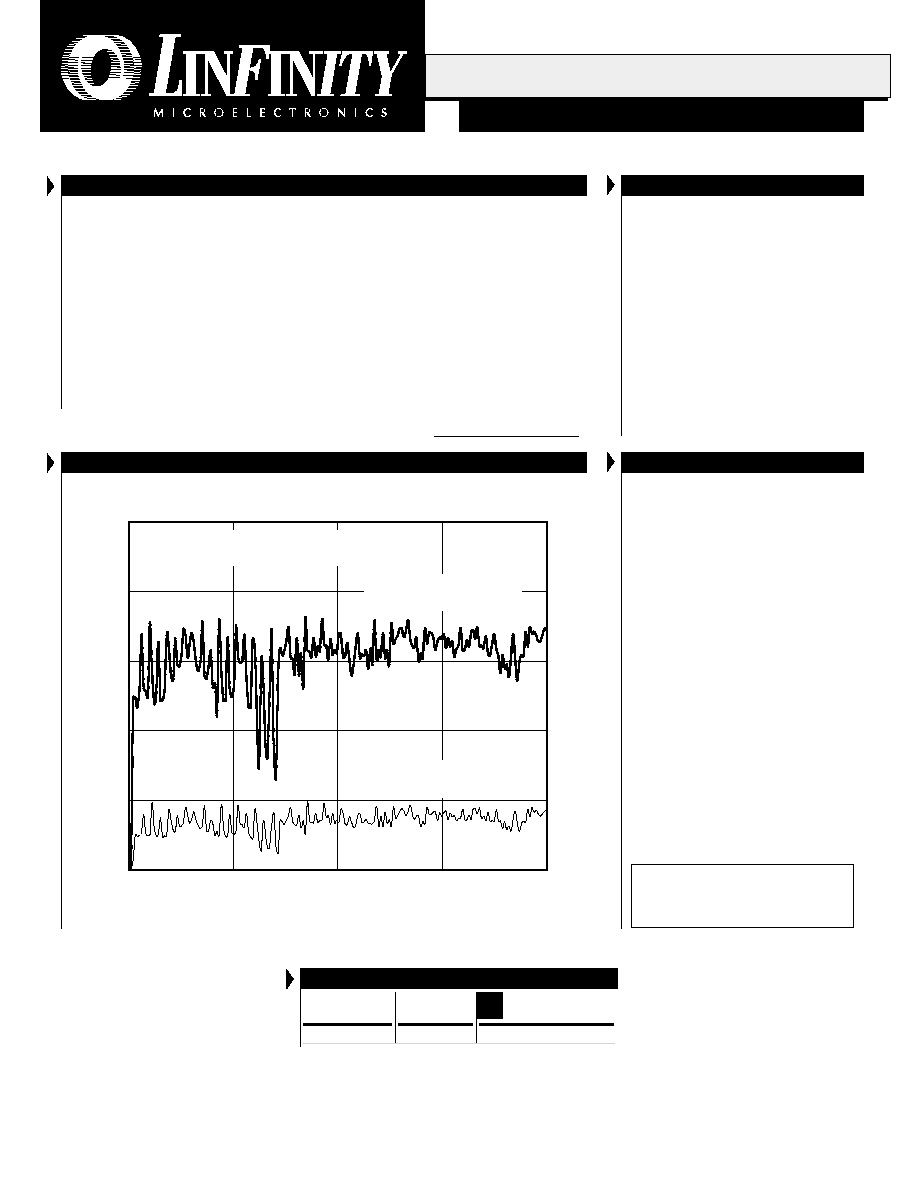
Highly Integrated
Linear Amplifier
Linfinity's LX1720
Class-D Amplifier
- Average Power Out for 20sec. approx. 512mW
- Across 8.6 Ohm Load
Audio sample from "Hold On Tight"
by Electric Light Orchestra
E
F F I C I E N C Y
C
O M PA R I S O N
O F
T H E
C
L A S S
-D A
M P L F I E R
Maximum
VDD
IMPORTANT: For the most current data, consult LinFinity's web site: http://www.linfinity.com.
APPLICATION NOTE AN-11
available on our web site
or call 1-800-LMI-7011
AudioMAX
TM
S
WITCHING
C
LASS
-D, S
TEREO
P
OWER
A
MPLIFIER
C
ONTROLLER
IC
LX1720
P R O D U C T D A T A B O O K 1 9 9 6 / 1 9 9 7
Copyright � 1999
Rev. 1.0 9/99
2
P
R O D U C T I O N
D
A T A
S
H E E T
AudioMAX
TM
A B S O L U T E M A X I M U M R A T I N G S
(Note 1)
Supply Voltage (PVDD, VDD) ...................................................................... -0.3V to 18V
RPWM .................................................................................................... -0.3V to V
CN
+0.3V
INPUT (R), INPUT (L) .......................................................................... -0.3V to V
CN
+0.3V
FBK+(R), FBK-(R), FBK+(L), FBK-(L), SLEEP .............................................. -0.3V to V
DD
MUTE (R), MUTE (L) .................................................................................... -0.3V to 6.0V
EAOUT (R), EAOUT (L) ....................................................................... -0.3V to V
CN
+0.3V
CPWM, CT ............................................................................................. -0.3V to V
CN
+0.3V
IS+, LIS-, RIS+ ................................................................................................ V
DD
-2 to V
DD
Operating Junction Temperature
Plastic (DB Package) ............................................................................................ 125�C
Storage Temperature Range ...................................................................... -65�C to 150�C
Lead Temperature (Soldering, 10 seconds) ............................................................ 300�C
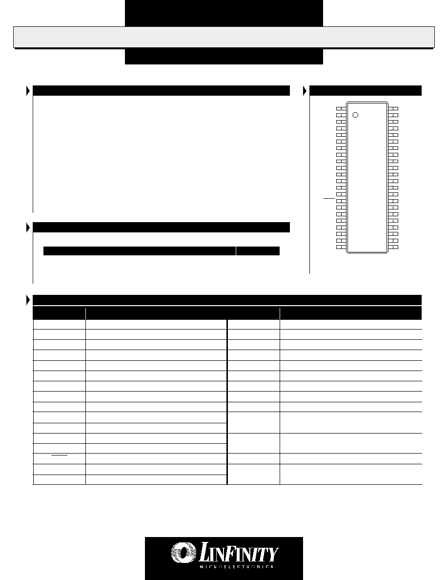
PACKAGE PIN OUTS
Note 1. Exceeding these ratings could cause damage to the device. All voltages are with
respect to Ground. Currents are positive into, negative out of the specified terminal.
DB PACKAGE:
THERMAL RESISTANCE-JUNCTION TO AMBIENT,
JA
65�C/W
Junction Temperature Calculation: T
J
= T
A
+ (P
D
x
JA
).
The
JA
numbers are guidelines for the thermal performance of the device/pc-board
system. All of the above assume no ambient airflow.
T H E R M A L D A TA
DB PACKAGE
(Top View)
FBK- (R)
FBK+ (R)
N.C.
VDD
CP
PVDD
PGND
P- (R)
N- (R)
N+ (R)
P+ (R)
P- (L)
N- (L)
N+ (L)
P+ (L)
PGND
PVDD
FBK- (L)
FBK+ (L)
GND
MUTE (L)
MUTE (R)
RIS-
LIS-
IS+
RPWM
CPWM
CN
N.C.
CT
RT
RBIAS
GND
AGND
INPUT (R)
INPUT (L)
SLEEP
EAIN (R)
N.C.
EAOUT (R)
FAOUT (R)
EAOUT (L)
EAIN (L)
FAOUT (L)
1
44
2
43
3
42
4
41
5
40
6
39
7
38
8
37
9
36
10
35
11
34
12
33
13
32
14
31
15
30
16
29
17
28
18
27
19
26
20
25
21
24
22
23
RIS-
LIS-
IS+
RPWM
CPWM
CN
CT
RT
RBIAS
GND
AGND
INPUT (R)
INPUT (L)
SLEEP
EAIN (R)
EAOUT (R)
Right Channel Current Sense Input
Left Channel Current Sense Input
Positive Current Sense Input
PWM Resistor Connection
PWM Capacitor Connection
Supply Decoupling for NFET Drivers
Oscillator Timing Capacitor Connection
Oscillator Timing Resistor
Bias Setting Resistor for Error Amps
Ground (2-pins)
Audio Input Ground
Right Channel Input
Left Channel Input
Sleep Input
Inverting Input of Right Channel Error Amp
Right Channel Error Amplifier Output
Pin Name
Description
F U N C T I O N A L P I N D E S C R I P T I O N
FAOUT (R)
EAOUT (L)
EAIN (L)
FAOUT (L)
FBK+(R), FBK-(R)
CP
PVDD
VDD
PGND
P+(R), N+(R),
P-(R), N-(R)
P+(L), N+(L),
P-(L), N-(L)
FBK+(L), FBK-(L)
MUTE (R),
MUTE (L)
Pin Name
Description
Output of Right Feedback Amp
Left Channel Error Amplifier Output
Inverting Input of Left Channel Error Amp
Output of Left Feedback Amp
Right Channel Feedback Inputs
Supply Decoupling for PFET Drivers
Output Driver Supply Voltage (2-pins)
Analog Supply Voltage
IC Power Ground for the Output Drivers (2-pins)
Right Channel Gate Drive Outputs
Left Channel Gate Drive Outputs
Left Channel Feedback Inputs
Mute Inputs
S
WITCHING
C
LASS
-D, S
TEREO
P
OWER
A
MPLIFIER
C
ONTROLLER
IC
LX1720
P R O D U C T D A T A B O O K 1 9 9 6 / 1 9 9 7
3
Copyright � 1999
Rev. 1.0 9/99
P
R O D U C T I O N
D
A T A
S
H E E T
AudioMAX
TM
E L E C T R I C A L C H A R A C T E R I S T I C S
(Unless otherwise specified, the following specifications apply over the operating ambient temperature 0�C
T
A
70�C.
Test conditions: RT = 30k, CT = 100pF, VDD = PVDD = 15V.)
Parameter
Symbol
Test Conditions
Input Offset Voltage
DC Open Loop Gain
Unity Gain Bandwidth
High Output Voltage
I
OUT
= -100�A
Low Output Voltage
I
OUT
= +100�A
Input Common Mode Range
Input Bias Current
Oscillator Section
Oscillator Frequency
Oscillator Peak Voltage
Oscillator Valley Voltage
Oscillator Max. Frequency
Voltage Stability
Temperature Stability
Input Amplifiers
Stage Gain
Set by Internal Resistors
Input Impedance
Units
LX1720
Min.
Typ.
Max.
280
330
380
kHz
2.5
V
200
mV
1
MHz
1
2
%
2
%
5
mV
60
dB
7
MHz
4
V
50
mV
1
5
V
1
�A
3.465
3.5
3.535
V/V
42
k
Error Amplifiers
Current Limit Comparators
Voltage Sense Threshold
Comparator Response Time
200
220
240
mV
500
nsec
PWM Comparators
CPWM Delay To Output
250
nsec
PWM Current Generator
CPWM Charge Current
RPWM = 75k
Impedance of Internal Discharge FET
75
�A
20
Feedback Amplifiers
High Output Voltage
I
OUT
= -250�A
Low Output Voltage
I
OUT
= +250�A
Common Mode Rejection
Input Common Mode Range
Input Impedance
Stage Gain
LX1720-01
Set by Internal Resistors
4
V
50
mV
70
dB
0
V
DD
V
388
k
89
91
93
mV/V
Output Drivers For The N-Channel MOSFETs
Ext. NFET Drivers, Low Level Voltage
V
OL
I
SINK
= 3mA
I
SINK
= 75mA
Ext. NFET Drivers, High Level Voltage
V
OH
I
SOURCE
= 3mA
I
SOURCE
= 75mA, CN = 5.2V (applied externally)
30
100
mV
1
1.5
V
30
100
mV
1
1.5
V
Output Drivers For The P-Channel MOSFETs
Ext. PFET Drivers, Low Level Voltage
V
OL
I
SINK
= 3mA
I
SINK
= 75mA
Ext. PFET Drivers, High Level Voltage
V
OH
I
SOURCE
= 3mA
I
SOURCE
= 75mA, CP = 5.2V (applied externally)
30
100
mV
1
1.5
V
30
100
mV
1
1.5
V
S
WITCHING
C
LASS
-D, S
TEREO
P
OWER
A
MPLIFIER
C
ONTROLLER
IC
LX1720
P R O D U C T D A T A B O O K 1 9 9 6 / 1 9 9 7
Copyright � 1999
Rev. 1.0 9/99
4
P
R O D U C T I O N
D
A T A
S
H E E T
AudioMAX
TM
E L E C T R I C A L C H A R A C T E R I S T I C S
(Continued)
Parameter
Symbol
Test Conditions
Units
LX1720
Min.
Typ.
Max.
Undervoltage Lockout Section
Start Threshold Voltage
UV Lockout Hysteresis
UVLO Delay To Output Enable
6.3
6.5
6.7
V
500
mV
976
clkcyc
Supply Current
Sleep Current
SLEEP Input = 0V, T
A
= 25�C
Operating Current
SLEEP Input = 2V, V
IN
= 15V, No MOSFETs Connected
Sleep To Output Enable
Sleep Threshold
20
�A
5
7
mA
976
clkcyc
1.2
1.45
1.6
V
Mute Section
Mute Threshold
1.6
1.7
1.8
V
S
WITCHING
C
LASS
-D, S
TEREO
P
OWER
A
MPLIFIER
C
ONTROLLER
IC
LX1720
P R O D U C T D A T A B O O K 1 9 9 6 / 1 9 9 7
5
Copyright � 1999
Rev. 1.0 9/99
P
R O D U C T I O N
D
A T A
S
H E E T
AudioMAX
TM
B L O C K D I A G R A M
U V L O
V R E F
B I A S
O S C
C T
R
S
Q
Q
P - ( R )
N - ( R )
P + ( R )
N + ( R )
C L K
O U T P U T
D R I V E R S
A N D
P R O T E C T I O N
C I R C U I T R Y
C N
V D D
R
S
Q
Q
E r r o r A m p
P - ( L )
N - ( L )
P + ( L )
N + ( L )
IS
+
RI
S
-
LI
S
-
V D D
S L E E P
R P W M
C P W M
I N P U T ( L )
F B K + ( L )
F B K - ( L )
E A O U T ( L )
P V D D
P G N D
C L K
C L K
C L K
V D D
R T
C P
V
R E G
F A O U T ( L )
E A I N ( L )
R B I A S
F e e d b a c k
A m p
M U T E ( L )
I n p u t A m p
E r r o r A m p
I N P U T ( R )
F B K + ( R )
F B K - ( R )
E A O U T ( R )
F A O U T ( R )
E A I N ( R )
F e e d b a c k
A m p
M U T E ( R )
I n p u t A m p
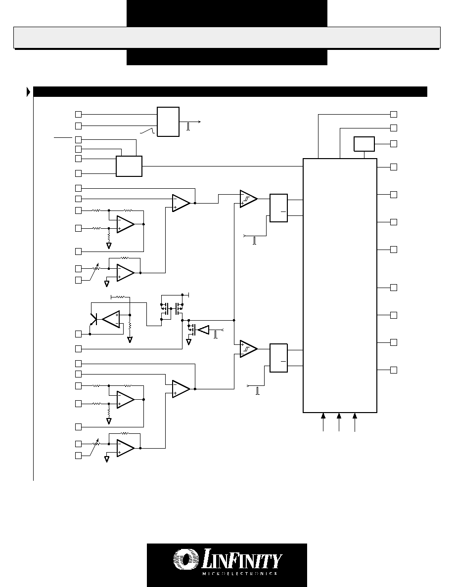
FIGURE 1 -- LX1720 Block Diagram
S
WITCHING
C
LASS
-D, S
TEREO
P
OWER
A
MPLIFIER
C
ONTROLLER
IC
LX1720
P R O D U C T D A T A B O O K 1 9 9 6 / 1 9 9 7
Copyright � 1999
Rev. 1.0 9/99
6
P
R O D U C T I O N
D
A T A
S
H E E T
AudioMAX
TM
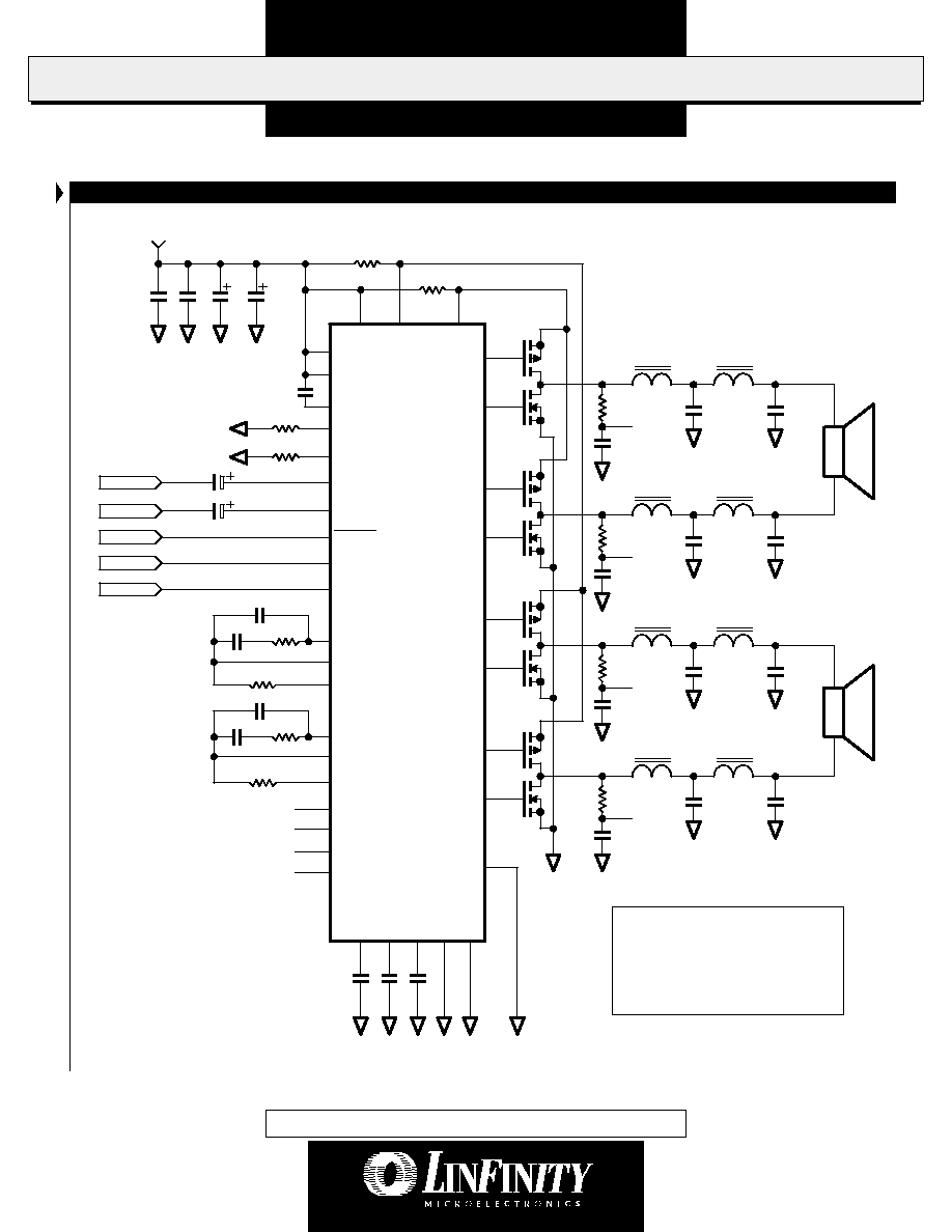
T Y P I C A L A P P L I C A T I O N
L
1
C
1 7
C
1 6
V
I N
= 7 V T O 1 5 V
L
2
C
1
R
1
F B K - ( R )
C
9
C
2
L
3
L
4
C
3
R
2
F B K + ( R )
C
1 0
C
4
L
5
L
6
C
5
R
3
F B K - ( L )
C
1 1
C
6
L 7
L 8
C
7
R
4
F B K + ( L )
C
1 2
C
8
Q
1
Q
2
Q
3
Q
4
Q
5
Q
6
Q
7
Q
8
R
5
R
6
PG
N
D
GN
D
A G N D
C
N
CN
C
T
C
PW
M
CP
W
M
C
1 8
C
1 9
F B K - ( R )
F B K + ( R )
F B K - ( L )
F B K + ( L )
F B K - ( R )
R
7
C
2 0
C
2 1
F A O U T ( R )
S L E E P
I N P U T ( L )
I N P U T ( R )
S L E E P
L E F T I N
R I G H T I N
C
2 4
C
2 5
R I S -
L I S -
I S +
L
X
1720
P - ( R )
N - ( R )
P + ( R )
N + ( R )
P - ( L )
P + ( L )
N + ( L )
CT
N - ( L )
P V D D
V D D
R P W M
R
P W M
RI
G
H
T
LE
FT
C P
R T
R
T
R M U T E
L M U T E
R M U T E
L M U T E
E A O U T ( R )
R
8
R
9
C
2 2
C
2 3
F A O U T ( L )
E A O U T ( L )
R
1 0
E A I N ( R )
E A I N ( L )
F B K + ( R )
F B K - ( L )
F B K + ( L )
C
P
FIGURE 2 -- Typical Class-D Stereo Switching Amplifier Circuit Application
For detailed application
information please refer to
APPLICATION NOTE AN-11
available on our web site
or call 1-800-LMI-7011
PRODUCTION DATA - Information contained in this document is proprietary to LinFinity, and is current as of publication date. This document
may not be modified in any way without the express written consent of LinFinity. Product processing does not necessarily include testing of
all parameters. Linfinity reserves the right to change the configuration and performance of the product and to discontinue product at any time.