 | –≠–ª–µ–∫—Ç—Ä–æ–Ω–Ω—ã–π –∫–æ–º–ø–æ–Ω–µ–Ω—Ç: LX1990ILM | –°–∫–∞—á–∞—Ç—å:  PDF PDF  ZIP ZIP |
Microsemi
Integrated Products
11861 Western Avenue, Garden Grove, CA. 92841, 714-898-8121, Fax: 714-893-2570
Page 1
Copyright
2001
Rev. 1.0c, 2002-05-29
WWW
.
M
i
c
r
o
sem
i
.
COM
LX1990
Dual Programmable
LED Current Sink
I N T E G R A T E D P R O D U C T S
D E S C R I P T I O N
D E S C R I P T I O N
D E S C R I P T I O N
D E S C R I P T I O N
The LX1990 is a dual output current
sink optimized for driving light emitting
diodes. This low cost bipolar IC enables
precise current regulation in LED
display lighting applications, yet
requires far fewer parts than discrete
solutions. The LX1990 is supplied in a
micro-miniature 6 lead MLP package
featuring a 3 x 3 mm footprint, a profile
of less than 1mm, and much improved
thermal performance. Its two output sink
currents are accurately matched and
require only one resistor to program.
Program current is only 1% of the
output currents, and quiescent current is
low, providing a very high efficiency
driver for battery-powered displays.
The LX1990 is based on a current-
mirror architecture that transfers a
reference current produced at the I
SET
pin to each of two open-collector current
sinking outputs. The output stages
multiply this reference current by 100 to
sink independently regulated currents up
to 30 mA.
Light output from LED's is proportional
to average current through them; they can
easily produce a brightness range of 500:1.
However, color of emitted light is shifted
by current amplitude. Color shift at low
light levels can be reduced by driving the
LED's with a constant peak current while
dimming with duty cycle control.
This is achieved by driving the I
SET
resistor with a PWM signal. A 500:1
brightness range can be achieved by
choosing 270 Hz as the PWM frequency (to
avoid optical beating with 50/60 Hz room
lights) and pulse width from 3.7
milliseconds to 7.4 microseconds.
The LX1990 features a shutdown mode
via the Enable pin. In this mode the
LX1990 consumes less than 1
µA and holds
the two open collector output stages off.
This pin may also be used to pulse width
modulate output current. See applications
section for dimming details.
IMPORTANT:
For the most current data, consult
MICROSEMI
's website: http://www.microsemi.com
K E Y F E A T U R E S
K E Y F E A T U R E S
K E Y F E A T U R E S
K E Y F E A T U R E S
∑
Programmable Sink Current
0.1 to 30mA x 2 Channels
∑
Replaces Discrete Transistor
Circuitry With A Single Package
∑
300mV Maximum Current Sink
Dropout Voltage at 20mA
∑
2.7 to 5.5V Power Supply Input
∑
I
OUT
Compliance Voltage from
0.1 to 10V
DC
∑
Enable Input With <1µA Sleep
Current
∑
Amplitude and PWM Dimming
∑
Current rise and fall time may
be controlled to reduce EMI
A P P L I C A T I O N S
A P P L I C A T I O N S
A P P L I C A T I O N S
A P P L I C A T I O N S
∑
Cell Phone Display Illumination
∑
PDA White LED Display
Lighting
∑
Automotive Display Illumination
∑
Digital Still Camera
∑
Camcorders
∑
Consumer Electronics Front
Panels
P R O D U C T H I G H L I G H T
P R O D U C T H I G H L I G H T
P R O D U C T H I G H L I G H T
P R O D U C T H I G H L I G H T
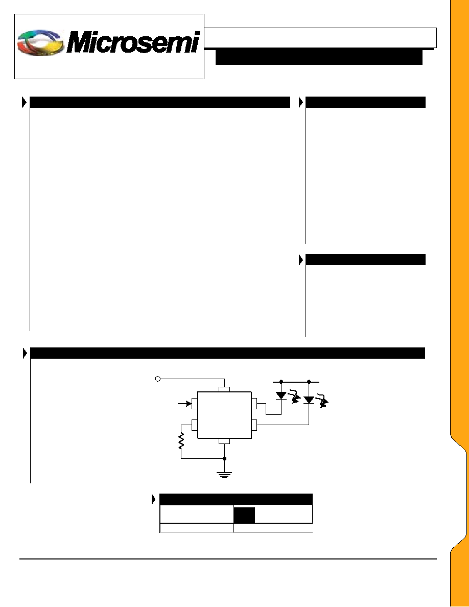
5V
LX1990
VDD
I
OUT B
GND
I
OUT A
ISET
R
SET
ENA
V
LOAD
ON/OFF
PACKAGE ORDER INFO
T
A
(
∞
∞
∞
∞C)
LM
Plastic MLP
6-Pin
-40 to 85
LX1990ILM
Note: Available in Tape & Reel.
Append the letter "T" to the part number. (i.e. LX1990ILM-T)
L
L
X
X
1
1
9
9
9
9
0
0
Microsemi
Integrated Products
11861 Western Avenue, Garden Grove, CA. 92841, 714-898-8121, Fax: 714-893-2570
Page 2
Copyright
2001
Rev. 1.0c, 2002-05-29
WWW
.
M
i
c
r
o
sem
i
.
COM
LX1990
Dual Programmable
LED Current Sink
I N T E G R A T E D P R O D U C T S
A B S O L U T E M A X I M U M R A T
A B S O L U T E M A X I M U M R A T
A B S O L U T E M A X I M U M R A T
A B S O L U T E M A X I M U M R A T I N G S
I N G S
I N G S
I N G S
Supply Voltage (V
DD
)........................................................................................ 6V
ENA Voltage ..................................................................................................... 6V
I
SET
Maximum Current ..............................................................Internally Limited
I
SET
Maximum Voltage...................................................................................
V
DD
I
OUT
Maximum Compliance Voltage............................................................... 12V
Current Source Outputs .............................................................................. 100mA
Operating Temperature Range......................................................... -40∞C to 85∞C
Maximum Junction Temperature..................................................................125∞C
Storage Temperature ..................................................................... -65∞C to 150∞C
Lead Temperature (Soldering, 10sec)........................................................... 300
∞C
Note: Exceeding these ratings could cause damage to the device. All voltages are with respect to
Ground. Currents are positive into, negative out of specified terminal
.
T H E R M A L D A T A
T H E R M A L D A T A
T H E R M A L D A T A
T H E R M A L D A T A
LM
Plastic MLP 6-Pin
THERMAL RESISTANCE
-
JUNCTION TO
A
MBIENT
,
JA
41
∞
∞
∞
∞
C/W
Junction Temperature Calculation: T
J
= T
A
+ (P
D
x
JA
).
The
JA
numbers are guidelines for the thermal performance of the device/pc-board
system. All of the above assume no ambient airflow.
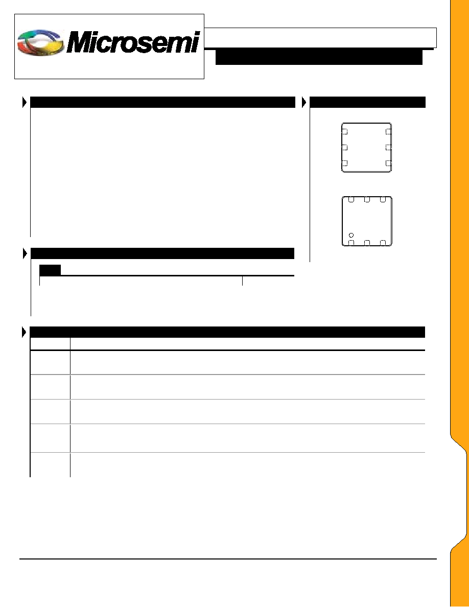
PACKAGE PIN OUT
PACKAGE PIN OUT
PACKAGE PIN OUT
PACKAGE PIN OUT
VDD
ENA
GND
I
OUTB
I
OUTA
ISET
1
2
3
4
5
6
LM P
ACKAGE
(Top View)
1990
xxxx
LMI
LM P
ACKAGE
M
ARKINGS
xxxx ≠ Denotes Date Code / Lot Identification
F U N C T I O N A L P I N D E S C R
F U N C T I O N A L P I N D E S C R
F U N C T I O N A L P I N D E S C R
F U N C T I O N A L P I N D E S C R I P T I O N
I P T I O N
I P T I O N
I P T I O N
N
AME
D
ESCRIPTION
V
DD
Input
Supply
GND Common
ground
reference
ENA
Chip Enable Input. If logic high, current source outputs are enabled. If logic low, internal power is disconnected
from the VDD pin, disabling all functions. Logic threshold is 1.2 V.
I
OUTA
&
I
OUTB
Output Current Source. Two separate constant current outputs. Outputs may be loaded in any combination
without affecting regulation of the loaded output. If only one output is needed I
OUTA
& I
OUTB
must be shorted
together. In this case the value of ISET resistor must be doubled. Compliance voltage range is 0.1V to 10V.
I
SET
Output current programming pin.
P
P
A
A
C
C
K
K
A
A
G
G
E
E
D
D
A
A
T
T
A
A
Microsemi
Integrated Products
11861 Western Avenue, Garden Grove, CA. 92841, 714-898-8121, Fax: 714-893-2570
Page 3
Copyright
2001
Rev. 1.0c, 2002-05-29
WWW
.
M
i
c
r
o
sem
i
.
COM
LX1990
Dual Programmable
LED Current Sink
I N T E G R A T E D P R O D U C T S
R E C O M M E N D E D O P E R A T I N
R E C O M M E N D E D O P E R A T I N
R E C O M M E N D E D O P E R A T I N
R E C O M M E N D E D O P E R A T I N G C O N D I T I O N S
G C O N D I T I O N S
G C O N D I T I O N S
G C O N D I T I O N S
LX1990
Parameter
Min Typ Max
Units
Supply Voltage (V
DD
) 2.7
5.5
V
ENA (ENABLE) Input Voltage
0
V
DD
V
I
SET
Voltage
0
1.25
V
I
SET
Current
0
300
µA
I
OUTA
/ I
OUTB
Compliance Voltage Range
0.1
10
V
I
OUTA
/ I
OUTB
Output Current Range
0.1
30
mA
E L E C T R I C A L C H A R A C T E R
E L E C T R I C A L C H A R A C T E R
E L E C T R I C A L C H A R A C T E R
E L E C T R I C A L C H A R A C T E R I S T I C S
I S T I C S
I S T I C S
I S T I C S
Unless otherwise specified, the following specifications apply over the operating ambient temperature -40
∞C
T
A
85
∞C and the
following test conditions: V
DD
= 2.7 to 5.5 V
DC
, I
SET
= 200µA
, V
OUT
5.5V, VLOAD
10V. Typical values are at T
A
= 25∞C
LX1990
Parameter Symbol
Test
Conditions
Min Typ Max
Units
Power Characteristics
Quiescent Current
I
_QUI
VDD = 2.7V; ISET = 0uA
1.4
2
mA
Quiescent Current
I
_QUI
VDD = 5.5V; ISET = 300uA
3.0
4
mA
Sleep Current
1
I
_SLEEP
VDD = 5.5V, ENA
0.4V
0.08 1 µA
Enable Input
Enable Logic Threshold
V
TH_EN
0.8 1.55 2.4 V
Enable Input Current
I
IN_EN
ENA
=
V
DD
= 5.5V
4
10
µA
I
SET
to Out Pulse Response
T
D(ON)
1.2 2 µS
I
SET
to Out Pulse Response
T
D(OFF)
1.4
2 µS
ISET Input
I
SET
Current Range
I
ISET
R
SET
terminated to GND
0
300
µA
I
SET
Voltage
V
ISET
I
SET
= 200uA
1.225
1.25
1.275
V
DC
Output Characteristics
Output Current Amplitude
I
OUT
0.5
<
V
OUT
< 5.5V, I
SET
= 200µA
18.5
20
21.5
mA
DC
OUTA to OUTB Current Matching
I
OUT_MATCH
I
OUT
= 20mA ; (I
OUTA
≠ I
OUTB
) / I
OUTA
* 100
0.4
5
%
ISET to IOUT Current Ratio
I
OUT_RATIO
I
OUT
/I
SET
; I
SET
= 200µA ; V
DD
= 5.5V
102
ISET to IOUT Current Ratio
I
OUT_RATIO
I
OUT
/I
SET
; I
SET
= 200µA ; V
DD
= 2.7V
99
Output Current I
SET
= 0µA
I
OUT_ZERO
0.5 < V
OUT
< V
LOAD
, I
SET
= 0µA
10
100
µA
DC
Dropout Voltage
2
V
DROPOUT
I
OUT
= 20mA
150
300
mV
Dropout Voltage
2
V
DROPOUT
I
OUT
= 30mA
200
400
mV
Maximum Output Current, I
SET
Shorted To Gnd. Each Output
I
SC
V
ISET
= Zero Volts; VDD=5V
100
mA
DC
Output Off State Current
I
OUTOFF
ENA
0.4V
20
µA
DC
1
At enable voltages greater than 0.4V but less than 0.8V the outputs will remain off but the sleep current may be greater than 1µA.
2
Dropout is defined as the OUTA/B to GND voltage at which the output current sink drops 10% from the nominal value.
E
E
L
L
E
E
C
C
T
T
R
R
I
I
C
C
A
A
L
L
S
S
Microsemi
Integrated Products
11861 Western Avenue, Garden Grove, CA. 92841, 714-898-8121, Fax: 714-893-2570
Page 4
Copyright
2001
Rev. 1.0c, 2002-05-29
WWW
.
M
i
c
r
o
sem
i
.
COM
LX1990
Dual Programmable
LED Current Sink
I N T E G R A T E D P R O D U C T S
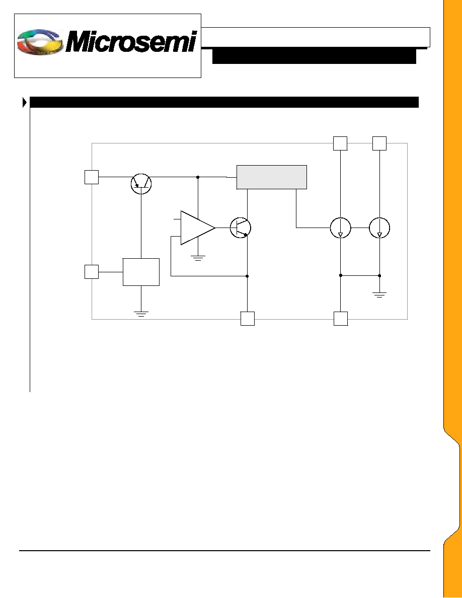
S I M P L I F I E D B L O C K D I A
S I M P L I F I E D B L O C K D I A
S I M P L I F I E D B L O C K D I A
S I M P L I F I E D B L O C K D I A G R A M
G R A M
G R A M
G R A M
VDD
ENABLE
+
-
ISET
1:1 Current Mirror
100X
100X
GND
I
OUTA
I
OUTB
1.25V
REF
Bias
Figure 1 ≠ Simplified Block Diagram
B
B
L
L
O
O
C
C
K
K
D
D
I
I
A
A
G
G
R
R
A
A
M
M

Microsemi
Integrated Products
11861 Western Avenue, Garden Grove, CA. 92841, 714-898-8121, Fax: 714-893-2570
Page 5
Copyright
2001
Rev. 1.0c, 2002-05-29
WWW
.
M
i
c
r
o
sem
i
.
COM
LX1990
Dual Programmable
LED Current Sink
I N T E G R A T E D P R O D U C T S
A P P L I C A T I O N S
A P P L I C A T I O N S
A P P L I C A T I O N S
A P P L I C A T I O N S
F
UNCTIONAL
D
ESCRIPTION
The LX1990 is designed to drive LED's used in display
illumination and signaling applications such as cellular
telephones and PDA's. With a 5V supply, the two
independently regulated constant current outputs can drive
2 white LED's (V
F
< 4.5V) in parallel, or 4 green or
amber LED's (V
F
< 2.25V each) arranged as 2 parallel x 2
in series.
With Dropout voltage of only 300 mV at 20 mA, the
LX1990 provides regulated current for 2 green / amber
LED's in a cell phone all the way down to the minimum
NiCd cutoff of 2.7 volts for three cells.
The LX1990 features resistor settable output current.
Connecting a resistor between I
SET
and a voltage of zero to
1.25 volts generates a current that is mirrored into each of
the output with a gain of about 100. Output current can be
varied in an analog fashion by varying I
SET
resistance or
termination voltage (see application schematics).
Duty cycle dimming with a fixed current amplitude is
accomplished by switching the I
SET
current on and off
with an open collector or open drain pulse width
modulated logic signal. Switching frequency can exceed
20 KHz, making it practical to use a PWM output channel
from popular micro controllers. The upper limit on
frequency is minimum switching response from I
SET
to
output. As frequency increases, these fixed delays will
cause an error in expected output current duty cycle.
All inputs and outputs are ESD and short circuit
protected making the LX1990 an exceptionally robust
component. However it is not recommended to
indefinitely short the I
SET
input to ground while shorting
the outputs to 10V as the power dissipation under these
conditions is the greatest.
A
PPLICATION
N
OTES
Each output has an independent current sink, however
both must be held above about 0.5 volts to maintain
specified current regulation accuracy. If only one output
is needed, the two outputs should be connected together
and the programming resistor value doubled so each
output supplies Ω the desired current. In this case, more
than 60 mA total current can be delivered from the
combined output.
Package power dissipation can be calculated from the
following equation:
(
) (
)
ED
LOAD
L
OUT
D
V
V
I
n
P
-
=
n
=
Number of outputs used
I
OUT
=
Current from each output
V
LOAD
=
Output Supply Voltage
V
LED
=
Minimum LED forward voltage
P
D
=
Power Dissipated in mW
When the ENA input is at zero volts, less than 20µA
current flows into or out of the outputs. If the disable
function is used , ENA must be driven below 0.4 volts to
insure minimum current from V
DD
.
The I
SET
pin may be driven with a digital open collector or
open drain logic PWM signal to dim the LED's.
Recommended PWM frequency for dimming is between
100 Hz and 20 KHz. Below 100 Hz flicker may be
observed. Above 20 KHz duty cycle accuracy is reduced due
to switching delays from I
SET
to outputs. Totem pole output
drive may also be used as long as the maximum driver
voltage never exceeds the V
DD
supply. Since the totem pole
drive will exceed the 1.25V I
SET
voltage it can introduce
delays that may limit the useful frequency and maximum
dim range.
If PWM dimming is used, use separate power and ground
lines directly from the power source point to prevent noise
generated from the LED current transients from entering
video or audio subsystems on the same supply rails.
Additional power supply filtering may be needed in PWM
dimming applications. Care should be exercised in the PCB
layout to prevent coupling from the outputs to the I
SET
pin,
as this may cause the part to oscillate.
Current out of the I
SET
pin may be varied for current
amplitude dimming. There are two ways to do this: If a
mechanical input is needed, a rheostat in series with a
resistor connected from GND to I
SET
can be used. The
second method is to connect a fixed resistor from I
SET
to the
output of a voltage DAC or other low impedance voltage
source. Varying the voltage between zero and 1.25 volts will
cause a corresponding output current change from I
OUT
max
to zero:
SET
OUT
I
Ratio
Current
I
◊
=
The ENA pin may be used to duty cycle dim the output
in applications where only one control line is available for
dimming and shutdown. A narrow current spike that may be
as high as 100 mA is produced when the ENA signal has
very fast rise times. This is not harmful to the LED, but will
cause dimming linearity errors when operating at very low
duty cycles.
A
A
P
P
P
P
L
L
I
I
C
C
A
A
T
T
I
I
O
O
N
N
S
S