Microsemi
Integrated Products Division
11861 Western Avenue, Garden Grove, CA. 92841, 714-898-8121, Fax: 714-893-2570
Page 1
Copyright
2000
Rev. 1.0, 2002-12-30
WWW
.
Microse
m
i
.
CO
M
LX1993
High Efficiency LED Driver
P
RODUCTION
I N T E G R A T E D P R O D U C T S
D E S C R I P T I O N
The LX1993 is a high efficiency
step-up boost converter that features a
psuedo-hysteretic pulse frequency
modulation topology for driving
white or color LEDs in backlight or
frontlight systems. Designed for
maximum efficiency, reduced board
size, and minimal cost, the LX1993 is
ideal for PDA and digital camera
applications. The LX1993 features an
internal N-Channel MOSFET and
control circuitry that is optimized for
portable system design applications.
The LX1993 promotes improved
performance in battery-operated
systems by operating with a quiescent
supply current 70�A (typical) and a
shutdown current of less than 1�A.
The input voltage range is from 1.6V
to 6.0V thus allowing for a broad
selection of battery voltage
applications and start-up is
guaranteed at 1.6V input.
The LX1993 is capable of switching
currents in excess of 300mA and the
output current is readily programmed
using one external current sense
resistor in series with the LEDs. This
configuration provides a feedback
signal to the FB pin thus maintaining
constant output current regardless of
varying LED forward voltage (V
F
).
The LX1993 provides an additional
feature for simple dynamic adjustment
of the output current (i.e., up to 100%
of the maximum programmed
current). Designers can make this
adjustment by generating an analog
reference signal or a PWM signal
applied directly to the ADJ pin and
any PWM amplitude is readily
accommodated via a single external
resistor. The LX1993 is available in
the 8-Pin MSOP and thus requires a
very small PCB area.
IMPORTANT: For the most current data, consult MICROSEMI's website: http://www.microsemi.com
K E Y F E A T U R E S
> 80% Maximum Efficiency
70�A Typical Quiescent Supply
Current
Externally Programmable Peak
Inductor Current Limit For
Maximum Efficiency
Logic Controlled Shutdown
< 1�A Shutdown Current
Dynamic Output Current
Adjustment Via Analog
Reference Or Direct PWM Input
8-Pin MSOP Package
APPLICATIONS
Pagers
Wireless Phones
PDAs
Handheld Computers
LED Driver
Digital Camera Displays
P R O D U C T H I G H L I G H T
LX1993
GND
FB
CS
SW
SHDN
IN
ADJ
OUT
ON OFF
Li-Ion
PACKAGE ORDER INFO
T
A
(
�
C)
DU
Plastic MSOP
8-Pin
0 to 70
LX1993CDU
Note: Available in Tape & Reel.
Append the letter "T" to the part number. (i.e. LX1993CDUT)
L
L
X
X
1
1
9
9
9
9
3
3

Microsemi
Integrated Products Division
11861 Western Avenue, Garden Grove, CA. 92841, 714-898-8121, Fax: 714-893-2570
Page 2
Copyright
2000
Rev. 1.0, 2002-12-30
WWW
.
Microse
m
i
.
CO
M
LX1993
High Efficiency LED Driver
P
RODUCTION
I N T E G R A T E D P R O D U C T S
A B S O L U T E M A X I M U M R A T I N G S
Supply
Voltage
(V
IN
)........................................................................ -0.3V to 7.0V
Feedback Input Voltage (V
FB
) ................................................ -0.3V to V
IN
+ 0.3V
Shutdown Input Voltage (V
SHDN
)........................................... -0.3V to V
IN
+ 0.3V
Adjust Input Voltage (V
ADJ
) .................................................... -0.3V to V
IN
+0.3V
Output Voltage (V
OUT
) ...................................................................... -0.3V to 25V
Switch Voltage (V
SW
)........................................................ -0.3V to (V
OUT
+ 1.0V)
Switch Current (I
SW
)............................................................................. 500mArms
Operating Junction Temperature ..................................................................150
�
C
Storage Temperature Range .......................................................... -65
�
C to 150
�
C
Lead Temperature (Soldering 180 seconds) .................................................235
�
C
Note: Exceeding these ratings could cause damage to the device. All voltages are with respect to
Ground. Currents are positive into, negative out of specified terminal
.
T H E R M A L D A T A
DU
Plastic MSOP 8-Pin
THERMAL RESISTANCE
-
JUNCTION TO
A
MBIENT
,
JA
206
�
C/W
THERMAL RESISTANCE
-
JUNCTION TO
C
ASE
,
JC
39
�
C/W
Junction Temperature Calculation: T
J
= T
A
+ (P
D
x
JC
).
The
JA
numbers are guidelines for the thermal performance of the device/pc-board
system. All of the above assume no ambient airflow.
PACKAGE PIN OUT
1
2
4
3
5
6
8
7
SW
FB
IN
GND
OUT
CS
ADJ
DU P
ACKAGE
(Top View)
SHDN
FRONT MARKING
�
pin 1 indicator
F U N C T I O N A L P I N D E S C R I P T I O N
N
AME
D
ESCRIPTION
IN
Unregulated IC Supply Voltage Input � Input range from +1.6V to +6.0V. Bypass with a 1
�
F or greater capacitor
for low voltage operation.
FB
Feedback Input � Connect to a current sense resistor between the load and GND to set the maximum output
current.
SHDN
Active-Low Shutdown Input � A logic low shuts down the device and reduces the supply current to <1
�
A.
Connect SHDN to V
CC
for normal operation.
SW
Inductor Switching Connection � Internally connected to the drain of a 28V N-channel MOSFET. SW is high
impedance in shutdown.
CS
Current-Sense Amplifier Input � Connecting a resistor between CS and GND sets the peak inductor current limit.
GND
Common terminal for ground reference.
ADJ
Output Current Adjustment Input � Provides the internal reference for the output current feedback. The signal
input can be either a PWM signal or analog voltage allowing a dynamic output current adjustment. The signal
should typically range from 500mV to GND, but is capable of an input up to V
IN
. Caution should be used not to
exceed the device output current rating.
OUT
Output Current - Adjustable up to 25mA. Load voltage should not exceed 25V.
P
P
A
A
C
C
K
K
A
A
G
G
E
E
D
D
A
A
T
T
A
A
1993
C
�
MSC

Microsemi
Integrated Products Division
11861 Western Avenue, Garden Grove, CA. 92841, 714-898-8121, Fax: 714-893-2570
Page 3
Copyright
2000
Rev. 1.0, 2002-12-30
WWW
.
Microse
m
i
.
CO
M
LX1993
High Efficiency LED Driver
P
RODUCTION
I N T E G R A T E D P R O D U C T S
E L E C T R I C A L C H A R A C T E R I S T I C S
Unless otherwise specified, the following specifications apply over the operating ambient temperature 0
�
C
T
A
70
�
C except where
otherwise noted and the following test conditions: V
IN
= 3V, V
FB
= 0.3V, V
ADJ
= 0.2V and SW pin has +5V through 39.2
, SHDN =
V
IN
and CS = GND.
LX1993
Parameter Symbol
Test
Conditions
Min Typ Max
Units
Operating Voltage
V
IN
1.6 6.0 V
Minimum Start-up Voltage
V
SU
T
A
= +25
�
C
1.6
V
Start-up Voltage Temperature
Coefficient
k
VST
Guaranteed; not tested
-2
mV/
�
C
Not
switching
70
100
�
A
Quiescent Current
I
Q
V
SHDN
< 0.4V
0.2
0.5
�
A
FB Threshold Voltage
V
FB
275 300 325 mV
FB Input Bias Current
I
FB
Switching V
ADJ
= 0.4V
-100 100
nA
ADJ Input Voltage Range
V
ADJ
0.0 V
IN
V
ADJ Input Bias Current
I
ADJ
V
ADJ
< 0.3V
-150 50 nA
Shutdown Input Bias Current
I
SHDN
V
SHDN
= 0V
-100 100
nA
Shutdown High Input Voltage
V
SHDN
1.6
V
Shutdown Low Input Voltage
V
SHDN
0.4
V
Current Sense Bias Current
I
CS
2
6
�
A
Minimum Peak Current
I
MIN
R
CS
= 0
85 155
mA
Internal NFET On-resistance
R
DS(ON)
T
A
= +25
�
C; I
SW
= 10mA; V
FB
= 1V
1.1
Switch Pin Leakage Current
I
LEAK
V
SW
= 25V
0.23
�
A
Maximum Switch Off-Time
t
OFF
V
FB
= 1V
100
300
500
ns
Diode Forward Voltage
V
F
T
A
= +25
�
C; I
F
= 150mA
1.0 V
Diode Reverse Current
I
R
T
A
= +25
�
C; V
R
= 25V
1.5
�
A
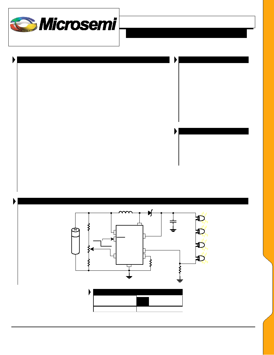
S I M P L I F I E D B L O C K D I A G R A M
Control
Logic
Reference
Logic
ADJ
FB
Shutdown
Logic
SHDN
CS
Driver
GND
SW
IN
4
�
A
OUT
2.5M
50pF
A1
A2
E
E
L
L
E
E
C
C
T
T
R
R
I
I
C
C
A
A
L
L
S
S
Microsemi
Integrated Products Division
11861 Western Avenue, Garden Grove, CA. 92841, 714-898-8121, Fax: 714-893-2570
Page 4
Copyright
2000
Rev. 1.0, 2002-12-30
WWW
.
Microse
m
i
.
CO
M
LX1993
High Efficiency LED Driver
P
RODUCTION
I N T E G R A T E D P R O D U C T S
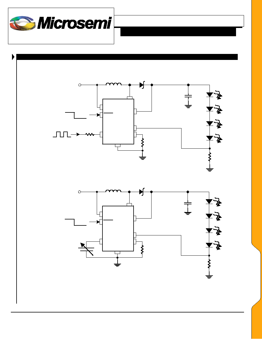
A P P L I C A T I O N C I R C U I T S
Typical LED Driver Applications
C
1
1
�
F
L
1
47
�
H
1206 Case Size
LX1993
GND
FB
CS
SW
SHDN
IN
ADJ
OUT
R
SET
1 5
V
BAT
= 1.6V to 6.0V
ON OFF
V
F
= 3.6V typ.
I
LED
= 20mA to 0mA
R
CS
1
k
Figure 1 � LED Driver with Full-Range Dimming Via PWM Input
C
1
1
�
F
L
1
47
�
H
1206 Case Size
LX1993
GND
FB
CS
SW
SHDN
IN
ADJ
OUT
R
S E T
15
V
BAT
= 1.6V to 6.0V
ON OFF
V
F
= 3.6V typ.
I
LED
= 20mA to 0mA
R
CS
1
k
V
ADJ
= 0.3V to 0.0V
+
-
Figure 2 � LED Driver with Full-Range Dimming Via Analog Voltage Input
Note: The component values shown are only examples for a working system. Actual values will vary greatly depending on
desired parameters, efficiency, and layout constraints.
A
A
P
P
P
P
L
L
I
I
C
C
A
A
T
T
I
I
O
O
N
N
S
S

Microsemi
Integrated Products Division
11861 Western Avenue, Garden Grove, CA. 92841, 714-898-8121, Fax: 714-893-2570
Page 5
Copyright
2000
Rev. 1.0, 2002-12-30
WWW
.
Microse
m
i
.
CO
M
LX1993
High Efficiency LED Driver
P
RODUCTION
I N T E G R A T E D P R O D U C T S
A P P L I C A T I O N I N F O R M A T I O N
O
PERATING
T
HEORY
The LX1993 is a PFM boost converter that is
optimized for driving a string of series connected LEDs. It
operates in a pseudo-hysteretic mode with a fixed switch
"off time" of 300ns. Converter switching is enabled as
LED current decreases causing the voltage across R
SET
to
decrease to a value less than the voltage at the VADJ pin.
When the voltage across R
SET
(i.e., V
FB
) is less than VADJ,
comparator A1 activates the control logic. The control
logic activates the DRV output circuit that connects to the
gate of the internal FET. The output (i.e., SW) is switched
"on" (and remains "on") until the inductor current ramps up
to the peak current level. This current level is set via the
external R
CS
resistor and monitored through the CS input by
comparator A2.
The LED load is powered from energy stored in the
output capacitor during the inductor charging cycle. Once
the peak inductor current value is achieved, the output is
turned off (off-time is typically 300ns) allowing a portion
of the energy stored in the inductor to be delivered to the
load (e.g., see Figure 6, channel 2). This causes the output
voltage to continue to rise across R
SET
at the input to the
feedback circuit. The LX1993 continues to switch until the
voltage at the FB pin exceeds the control voltage at the
ADJ pin. The value of R
SET
is established by dividing the
maximum adjust voltage by the maximum series LED
current. A minimum value of 15
is recommended for
R
SET
. The voltage at the FB pin is the product of I
OUT
(i.e.,
the current through the LED chain) and R
SET
.
=
LEDmax
ADJmax
I
V
R
SET
The application of an external voltage source at the
ADJ pin provides for output current adjustment over the
entire dimming range and the designer can select one of
two possible methods. The first option is to connect a
PWM logic signal to the ADJ pin (e.g., see Figure 1). The
LX1993 includes an internal 50pF capacitor to ground that
works with an external resistor to create a low-pass filter
(i.e., filter out the AC component of a pulse width
modulated input of f
PWM
100KHz). The second option is
to adjust the reference voltage directly at the ADJ pin by
applying a DC voltage from 0.0 to 0.3V (e.g., see Figure
2). The adjustment voltage level is selectable (with limited
accuracy) by implementing the voltage divider created
between the external series resistor and the internal 2.5M
resistor. Disabling the LX1993 is achieved by driving the
SHDN pin with a low-level logic signal thus reducing the
device power consumption to approximately 0.5
�
A (typ).
I
NDUCTOR
S
ELECTION AND
O
UTPUT
C
URRENT
L
IMIT
P
ROGRAMMING
Setting the level of peak inductor current to approximately
2X the expected maximum DC input current will minimize
the inductor size, the input ripple current, and the output
ripple voltage. The designer is encouraged to use inductors
that will not saturate at the peak inductor current level. An
inductor value of 47
�
H is recommended. Choosing a lower
value emphasizes peak current overshoot while choosing a
higher value emphasizes output ripple voltage. The peak
switch current is defined using a resistor placed between the
CS terminal and ground and the I
PEAK
equation is:
(
)
CS
SCALE
D
IN
MIN
PEAK
R
I
t
L
V
I
I
+
+
=
The maximum I
PEAK
value is limited by the I
SW
value
(max. = 500mA rms). The minimum I
PEAK
value is defined
when R
CS
is zero. The minimum I
PEAK
value is defined when
R
CS
is zero. A typical value for the minimum peak current
(I
MIN
) at 25
o
C is 197mA. The parameter t
D
is related to
internal operation of comparator A. A typical value at 25
o
C
is 850ns. A typical value of I
SCALE
at 25
o
C is 44mA per K
.
All of these parameters have an effect on the final I
PEAK
value.
D
ESIGN
E
XAMPLE
:
Determine I
PEAK
where V
IN
equals 3.0V and R
CS
equals
4.02K
using nominal values for all other parameters.
(
)
4.02K
k
44mA
0ns
5
8
47�7
3.0V
197mA
I
PEAK
�
+
�
+
=
The result of this example yields a nominal I
PEAK
of
approximately 428mA.
O
UTPUT
R
IPPLE AND
C
APACITOR
S
ELECTION
Output voltage ripple is a function of the inductor value
(L), the output capacitor value (C
OUT
), the peak switch
current setting (I
PEAK
), the load current (I
OUT
), the input
voltage (V
IN
) and the output voltage (V
OUT
) for a this boost
converter regulation scheme. When the switch is first turned
on, the peak-to-peak voltage ripple is a function of the output
droop (as the inductor current charges to I
PEAK
), the feedback
transition error (i.e., typically 10mV), and the output
overshoot (when the stored energy in the inductor is
delivered to the load at the end of the charging cycle).
Therefore the total ripple voltage is
V
RIPPLE
=
V
DROOP
+
V
OVERSHOOT
+ 10mV
The initial droop can be estimated as follows where the
0.5V value in the denominator is an estimate of the voltage
drop
across the inductor and the FET RDS_ON:
A
A
P
P
P
P
L
L
I
I
C
C
A
A
T
T
I
I
O
O
N
N
S
S