 | –≠–ª–µ–∫—Ç—Ä–æ–Ω–Ω—ã–π –∫–æ–º–ø–æ–Ω–µ–Ω—Ç: LX2173CP | –°–∫–∞—á–∞—Ç—å:  PDF PDF  ZIP ZIP |
LIN D
O C
#: 2172
D E S C R I P T I O N
K E Y F E A T U R E S
s 1.25A, 65V Internal Power Switch
s 3V - 25V Input Voltage Range
s Current-Mode Operation
s Improved Internal Cycle-By-Cycle Current
Limiting
s Thermal Shutdown
s Less Than 10µA Quiescent Current In
Microprocessor Shutdown Mode
s External Frequency Synchronization
Possible
s 100kHz Operating Frequency
The LX2172/73 are fixed-frequency, cur-
rent-mode switching regulator integrated
circuits. These ICs contain all necessary
control circuitry plus a 1.25A on-board
transistor to design a complete DC:DC
switching regulator with minimum exter-
nal components.
All functions are integrated into a single
IC, available in 8-pin DIP and SOIC or a
5-pin TO-220 power package, making
them extremely easy to design with and
use. The LX2172/73 are optimized for
boost and flyback applications, but can
also be used in forward and inverting
converter configuations.
The LX2172 can be connected to an
external clock for synchronization, and
can enter micropower operation when
the V
C
pin is pulled low. The LX2173
has an enable function, which permits
extremely low micropower operation,
consuming under 10µA current when the
ENABLE pin is brought low.
P R O D U C T H I G H L I G H T
A P P L I C A T I O N S
s Boost Converter
s Laptop / Notebook Computers
s Portable Equipment
s Small Motor Applications
s Flyback Converters
1.25A H
IGH
-E
FFICIENCY
100
K
H
Z
S
WITCHING
R
EGULATOR
P
R E L I M I N A R Y
D
A T A
S
H E E T
T
H E
I
N F I N I T E
P
O W E R
O F
I
N N O V A T I O N
LX2172/73
Note: All surface-mount packages are available in Tape & Reel.
Append the letter "T" to part number. (i.e. LX217xCDMT)
P A C K A G E O R D E R I N F O R M A T I O N
T
A
(∞C)
Plastic DIP
8-pin
0 to 70
LX217xCM
LX217xCDM
LX217xCP
M
Plastic SOIC
8-pin
DM
Plastic TO-220
5-pin
P
LX2172
SYNC Input
LX2173
Low µPower Mode
(HI ENABLE)
Part #
Pin 4
Connections
A
VA I L A B L E
O
P T I O N S
P E R
P
A R T
#
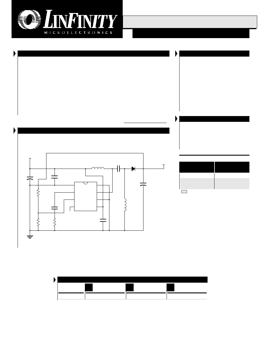
SEPIC C
O N V E R T E R
U
S I N G
T
H E
LX2172
Input 6-24V, Output 7V, 300mA
= Samples Not Yet Available.
L1
LX2172
D1
E
2
V
C
FB
SYNC
GND
V
SW
E
1
V
IN
1mH
1
2
3
4
8
7
6
5
U1
R
3
100
R
2
3.0k
C
4
0.47µF
(See Note 1)
R
1
13.7k
C
1
22µF
V
IN
6-24V
DC
C
DECOUPLE
0.47µF
1N5817
L2
1mH
C
OUT
220µF
7V
Output
7V
300mA
C
3
0.1µF
C
2
330µF
Note 1: SYNC Pin Requirements:
A) F
MAX
= 200kHz
B) TTL Compatible Level
C) Pulse Width T
P
Range - 0.1µs < T
P
< 2.0µs
Copyright © 1998
Rev. 0.4 12/98
1
11861 W
ESTERN
A
VENUE
, G
ARDEN
G
ROVE
, CA. 92841, 714-898-8121, F
AX
: 714-893-2570
L
I N
F
I N I T Y
M
I C R O E L E C T R O N I C S
I
N C
.
NOTE: For current data & package dimensions, visit our web site: http://www.linfinity.com.
1.25A H
IGH
-E
FFICIENCY
100
K
H
Z
S
WITCHING
R
EGULATOR
LX2172/73
P R O D U C T D A T A B O O K 1 9 9 6 / 1 9 9 7
Copyright © 1998
Rev. 0.4 12/98
2
P
R E L I M I N A R Y
D
A T A
S
H E E T
ABSOLUTE MAXIMUM RATINGS
(Note 1)
Supply Voltage (V
IN
) .................................................................................................... 25V
Collector Supply Voltage (V
C
) ..................................................................................... 65V
Digital Inputs (SYNC) ......................................................................................... -0.3 to 7V
Operating Junction Temperature ................................................................. 0∞C to 125∞C
Storage Temperature Range .................................................................... -65∞C to +150∞C
Solder Temperature (Soldering, 10 seconds) .......................................................... 300∞C
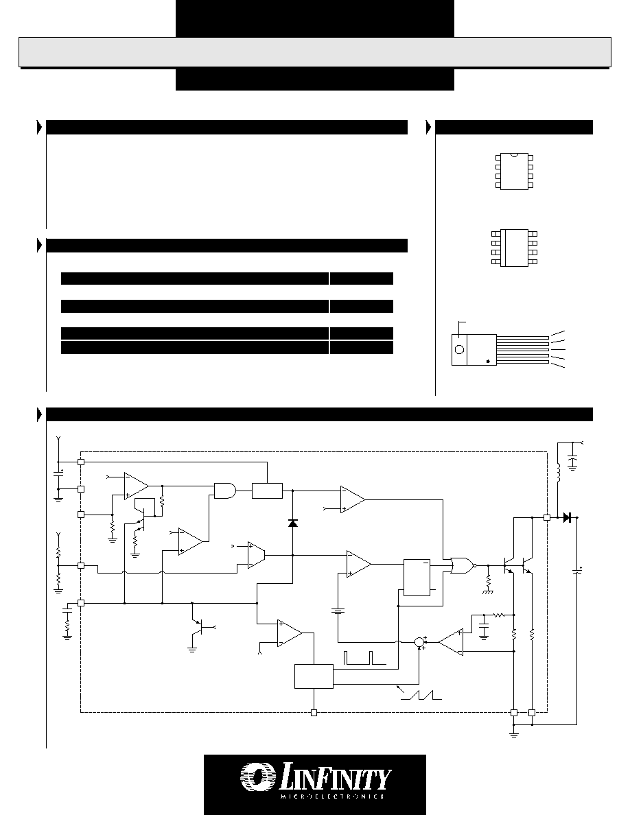
PACKAGE PIN OUTS
E
2
V
SW
E
1
V
IN
GND
V
C
FB
* SYNC / ENABLE
1
8
2
7
3
6
4
5
M PACKAGE
(Top View)
DM PACKAGE
(Top View)
E
2
V
SW
E
1
V
IN
GND
V
C
FB
* SYNC / ENABLE
1
8
2
7
3
6
4
5
Note 1. Exceeding these ratings could cause damage to the device. All voltages are with respect
to Ground. Currents are positive into, negative out of the specified terminal.
THERMAL DATA
M PACKAGE:
THERMAL RESISTANCE-JUNCTION TO AMBIENT,
JA
95∞C/W
DM PACKAGE:
THERMAL RESISTANCE-JUNCTION TO AMBIENT,
JA
165∞C/W
P PACKAGE:
THERMAL RESISTANCE-JUNCTION TO TAB,
JT
4.5∞C/W
THERMAL RESISTANCE-JUNCTION TO AMBIENT,
JA
60∞C/W
Junction Temperature Calculation: T
J
= T
A
+ (P
D
x
JA
).
The
JA
numbers are guidelines for the thermal performance of the device/pc-board system.
All of the above assume no ambient airflow.
V
IN
V
SW
GND
FB
V
C
P PACKAGE
(Top View)
1
5
TAB IS GND
* Pin 4 = SYNC for LX2172, ENABLE for LX2173/2174
5
1
3
2
7
6
8
V
I N
G N D
E N A B L E
F
B
V
C
S Y N C
E 1
E 2
S
W
1 0 0 k H z
O S C
I N
2 5 0 m V
1 . 4 V
C . S .
A M P
0.
16W
0.
16W
Q 1
Q 2
R
S
Q
Q
P W M
C O M P
P W M
L A T C H
0 . 1 5 V
S . D .
C O M P
E . A .
1 . 2 7 V
g
M
1 . 4 V
E N A B L E
C O M P
E N
2 . 3 V
V
R E G
V
R E G
U V L O C O M P
E N
V
I N
V
I N
V
O
( N O T E 1 )
( N O T E 1 )
V
O F S
( 0 . 9 V )
V
O
2 . 3 V
V
R E G
S L O P E C O M P
1 0 0 k H z
Note 1: LX2172 Only: SYNC brought out to pin 4. ENABLE is tied to V
IN
. LX2173 Only: ENABLE brought out to pin 4. SYNC is open.
B L O C K D I A G R A M
1.25A H
IGH
-E
FFICIENCY
100
K
H
Z
S
WITCHING
R
EGULATOR
LX2172/73
P R O D U C T D A T A B O O K 1 9 9 6 / 1 9 9 7
3
Copyright © 1998
Rev. 0.4 12/98
P
R E L I M I N A R Y
D
A T A
S
H E E T
E L E C T R I C A L C H A R A C T E R I S T I C S
Reference Section
Parameter
Symbol
Test Conditions
Initial Accuracy
V
REF
T
J
= 25∫C, Measured at FB pin
Over Temperature, Measured at FB pin
Line Regulation
3V < V
CC
< 25V
Units
LX2172 / 2173
Min.
Typ.
Max.
1.224
1.244
1.264
V
1.214
1.244
1.274
V
0.03
% / V
Error Amplifier Section
Input Bias Current
I
B
T
J
= 25∫C; V
FB
= V
REF
Over Temperature
Open Loop Gain
A
VOL
Transconductance
g
m
T
J
= 25∫C; V
FB
= V
REF
;
I = ±25µA
Over Temperature
Output Sink Current
I
EA (SINK)
Output Source Current
I
EA (SOURCE)
Output HI Voltage
V
COMP-HI
V
FB
= 1V
Output LO Voltage
V
COMP-LO
V
FB
= 1.5V
Slew Rate
S
350
750
nA
1100
nA
500
1000
V / V
3000
4400
6000
µMHO
2400
7000
µMHO
120
200
µA
120
µA
1.8
2.1
2.3
V
0.2
0.3
0.52
V
2
V/µsec
(Unless otherwise specified, these specifications apply over the ranges T
A
= 0 to 70∫C for the LX217xC. V
IN
= V
C
= 5V. All devices must be functional over
junction temperature of -65∞C to 150∞C. Typ. number represents T
A
= 25∫C value.)
Input Supply Section
Start-Up Threshold
Normal Mode Quiescent Current
I
Q
ENABLE = HI, V
C
= 0.6V, I
O
= 0A
V
C
Shutdown Threshold
3V < V
IN
< V
MAX
, T
J
= 25∞C
3V < V
IN
< V
MAX
, Over Temperature
Sleep Mode Current
ENABLE = HI, V
C
= 50mV
ENABLE = LO (LX2173 only)
2.2
2.7
2.9
V
5
8
mA
100
150
260
mV
50
300
mV
100
µA
5
µA
Oscillator Section
Switching Frequency
f
T
A
= 25∫C
Over Temperature
Line Voltage Stability
V
IN
= 3V to 25V
90
100
110
kHz
85
100
115
kHz
±5
%
Output Switch Breakdown Voltage
I
SW
= 1.5mA
Output Switch On Resistance
R
ON
I
O
= 2A
Switch Current Limit
I
LIM
D.C = 50%
50% < D.C < 80%
Total Switching Loss (On Time + Off Time)
V
IN
= 25V, D.C = 50%, I
O
= 1A, V
SW
= 60V
0.6
1.2
1.25
V
36
40
%
80
90
98
%
E.A. Output to PWM Drive Offset (VPWM)
V
OFS
Duty Cycle = 0
Minimum Duty Cycle
Maximum Duty Cycle
65
V
0.4
0.6
1.25
1.7
2.8
A
1.0
1.5
2.0
A
100
mW
PWM Section
Output Drive Section
100
ns
2
A / V
C.S. Delay to Driver Output
10% Over drive GBNT
V
C
to Output Transconductance
C.S. Comparator Section
1.25A H
IGH
-E
FFICIENCY
100
K
H
Z
S
WITCHING
R
EGULATOR
LX2172/73
P R O D U C T D A T A B O O K 1 9 9 6 / 1 9 9 7
Copyright © 1998
Rev. 0.4 12/98
4
P
R E L I M I N A R Y
D
A T A
S
H E E T
GND
1
3
V
C
2
1
FB
3
2
SYNC
4
ENABLE
4
V
IN
5
5
E
1
6
V
SW
7
4
E
2
8
Signal ground. Keep separate from power grounds (E
1
and E
2
).
Output of transconductance error amplifier. An R-C compensation network is connected from
this pin to the ground to stabilize the feedback loop. If this pin is pulled lower than 0.15V, the
IC goes into micropower mode.
Error amplifier inverting input. A resistor divider from the output of the converter to this pin sets
its nominal voltage.
LX2172 only. This pin is used to synchronize the device directly with a logic level input pulse.
External synchronization frequency must always be at a higher frequency than the minimum
internal clock. When not used, should be left open.
LX2173 only. This pin is the input to the enable comparator. A voltage under 1.4V will put the
device in micropower mode. Pin must be connected to V
IN
when not in use.
Input supply voltage (3.0V to 25V).
Power return of first transistor (Q
1
). This pin must be connected to ground.
Collector of output transistors. Connect to external inductor or input voltage, depending on circuit
topology.
Grounding this pin sets the current limit point to the maximum value. If pin is left open, the current
limit is set to half its maximum value.
Pin
Pin #
Pin #
Name
(8-pin Pkgs.) (5-pin TO-220)
Description
F U N C T I O N A L P I N D E S C R I P T I O N
F U N C T I O N A L P I N D E S C R I P T I O N
F U N C T I O N A L P I N D E S C R I P T I O N
F U N C T I O N A L P I N D E S C R I P T I O N
F U N C T I O N A L P I N D E S C R I P T I O N
E L E C T R I C A L C H A R A C T E R I S T I C S
Parameter
Symbol
Test Conditions
Units
LX2172 / 2173
Min.
Typ.
Max.
0.2
2
µsec
2
6
V
0.7
V
100
400
µA
1
5
µA
SYNC Pulse Width
SYNC Input HI
SYNC Input LO
SYNC Input Current HI
Input = 2V
SYNC Input Current LO
Input = 0.4V
SYNC Input Section (LX2172 only)
0.4
1.2
2.4
V
200
µA
100
µA
Enable Input Threshold
HI Input Current
Input = 2.4V
LO Input Current
Input = 0.4V
ENABLE Section (LX2173 only)
1.25A H
IGH
-E
FFICIENCY
100
K
H
Z
S
WITCHING
R
EGULATOR
LX2172/73
P R O D U C T D A T A B O O K 1 9 9 6 / 1 9 9 7
5
Copyright © 1998
Rev. 0.4 12/98
P
R E L I M I N A R Y
D
A T A
S
H E E T
T H E O R Y O F O P E R A T I O N
IC OPERATION
Referring to the block diagram, when V
IN
is above the UVLO
start threshold the 2.3V UVLO comparator output switches to
low state, allowing Q1 to turn on upon receiving a clock pulse
from the internal 100kHz oscillator. Once Q1 is on, current in
the inductor ramps up. Inductor current is then sensed, and
amplified by a current sense amplifier and compared to a thresh-
old set by the output of the error amplifier minus the offset
voltage (V
OFS
typically 0.9V). This allows the PWM comparator
to reset the flip flop, causing Q1 to turn off. The oscillator then
sets the flip flop, and the operation repeats itself.
CURRENT LIMIT
Current limiting is performed by sensing the peak switch cur-
rent and turning Q1 off until the next clock cycle. When the
converter goes into current limit the error amplifier output goes
to the rail and sets a maximum limit on the current.
ERROR AMPLIFIER
The function of the error amplifier is to set a threshold voltage
for inductor peak current and control the switch duty cycle so
that the power supply output voltage is closely regulated. Regu-
lation is accomplished by sensing the output voltage and com-
paring it to the internal 1.27V bandgap reference. A compensa-
tion network is placed from the output of the amplifier to ground
for closed loop stability purposes, as well as a high d.c. gain for
tight regulation. The function of V
OFS
is to keep Q1 off without
requiring an error amplifier output to swing to ground level. It
is required the V
OL
of the error amplifier is always less than the
offset at all times. The transfer function between the error
amplifier output (V
C
) and peak inductor current is therefore
given by:
V
C
- V
OFS
= I
P
* G * R
S
Where: I
P
= Inductor peak current
G = Current sense gain (typically 6)
R
S
= Internal sense resistor
OSCILLATOR
The oscillator is designed to operate at 100kHz frequency. Its
function is to turn the switch Q1 on at a fixed 10µs interval and
to provide a slope compensation for the feedback loop. Slope
compensation is required for fixed frequency continuous Cur-
rent Mode regulators operating above 50% duty cycle in order
to prevent loop instability. The SYNC input is a logic input that
allows easy synchronization to an external clock. Synchroniza-
tion is done such that the external clock terminates the cycle
before the internal oscillator sets the PWM latch again.
UNDER-VOLTAGE LOCKOUT
The 2.3V internal regulator is monitored as the input supply
ramps up, ensuring glitch-free operation.
EXTRA PINS ON 8-PIN DEVICE
The 8-pin versions of the LX217x have the emitters of the power
transistors brought out separately. Connecting these pins to
ground reduces errors due to ground pin voltage drops. The E
2
pin also allows the user to half the switch current limit if the pin
is left open. Note that the switch resistance will increase when
E
2
is open, so efficiency will decrease and heat dissipation will
increase, especially for currents over 300mA.
MICROPOWER SHUTDOWN
The LX2172/73 enter micropower shutdown mode when the V
C
pin is pulled below 0.15V. Supply current required for biassing
shutdown circuitry is less than 250µA. The LX2173 has an EN-
ABLE pin which allows ultra-low micropower shutdown opera-
tion, consuming less than 10µA.