
0 to 70
LX5111ACDP
LX5111ACPWP
LX5112ACDP
LX5112ACPWP
U L T R A 9 - C
H A N N E L
S C S I T
E R M I N A T O R
P
R E L I M I N A R Y
D
A T A
S
H E E T
T
H E
I
N F I N I T E
P
O W E R
O F
I
N N O V A T I O N
LX5111A/5112A
LIN D
O C
#: 51115
D E S C R I P T I O N
K E Y F E A T U R E S
s Ultra-Fast Response For FAST-20 SCSI
Applications
s 35MHz Channel Bandwidth
s 3.0V Operation
s Less Than 3pF Output Capacitance
s Thermally Self-Limiting
s NO External Compensation Capacitors
s Implements 8-bit Or 16-bit (Wide)
Applications
s Compatible with Active Negation
Drivers
s Compatible With Passive And Active
Terminations
s Approved For Use With SCSI 1, 2, 3
And Ultra SCSI
s Hot-Swap Compatible
s Pin-For-Pin Compatible With
LX5211 and UC5606 (LX5111)
s Pin-For-Pin Compatible With
LX5212 And UC5603/5613/5614
(LX5112)
Receiver
LX5111A/5112A
LX5268
LX5268
1 Meter, AWG 28
Driver
LX5111A/5112A
D
R I V I N G
W
AV E F O R M
- 20MH
Z
R
E C E I V I N G
W
AV E F O R M
- 20MH
Z
P R O D U C T H I G H L I G H T
The LX5111A/5112A SCSI terminators are part of
Linfinity's UltraMAX family of high-performance,
adaptive, non-linear mode SCSI products, which
are designed to deliver true UltraSCSI performance
in SCSI applications. The low voltage BiCMOS
architecture employed in their design offers su-
perior performance to older linear passive and
active techniques. Linfinity's UltraMAX architecture
employs high-speed adaptive elements for each
channel, thereby providing the fastest response
possible -- typically 35MHz, which is 100 times
faster than the older linear regulator/terminator
approach used by other manufacturers. Products
using this older linear regulator approach have
bandwidths which are dominated by the output
capacitor and which are limited to 500KHz (see
further discussion in the Functional Description
section). The UltraMAX architecture also eliminates
the output compensation capacitor typical in earlier
terminator designs. Each is approved for use with
SCSI-1, -2, -3, UltraSCSI and beyond -- providing
the highest performance alternative available to-
day.
Another key improvement offered by the
LX5111A/12A lies in their ability to insure reliable,
error-free communications even in systems which
do not adhere to recommended SCSI hardware
design guidelines, such as the use of improper
cable lengths and impedances. Frequently, this
situation is not controlled by the peripheral or host
designer and, when problems occur, they are the
first to be made aware of the problem. The
LX5111A/12A architecture is much more tolerant
of marginal system integrations.
Recognizing the needs of portable and
configurable peripherals, the LX5111A/12A have
a TTL compatible sleep/disable mode. Quiescent
current is typically less than 275µA in this mode,
while the output capacitance is also less than 3pF.
The obvious advantage of extended battery life
for portable systems is inherent in the product's
sleep-mode feature. Additionally, the disable
function permits factory-floor or production-line
configurability, reducing inventory and product-
line diversity costs. Field configurability can also
be accomplished without physically removing
components which, often times results in field
returns due to mishandling.
Reduced component counts is also inherent in
the LX5111A/12A's architecture. Traditional ter-
mination techniques require large stabilization and
transient protection capacitors of up to 20µF in
value and size. The LX5111A/12A architecture
does not require these components, allowing all
the cost savings associated with inventory, board
space, assembly, reliability, and component costs.
NOTE:
For An In-Depth
Discussion On Applying
SCSI, Request Linfinity
Application Note:
"Understanding The Single-
Ended SCSI Bus"
UltraMAX
TM
P A C K A G E O R D E R I N F O R M A T I O N
T
A
(∞C)
Note: All surface-mount packages are available in Tape & Reel.
Append the letter "T" to part number. (i.e. LX5111ACDPT)
Plastic SOIC
16-pin, Power
DP
PWP
Plastic TSSOP
24-pin, Power
Copyright © 1999
Rev. 0.1 3/99
1
11861 W
ESTERN
A
VENUE
, G
ARDEN
G
ROVE
, CA. 92841, 714-898-8121, F
AX
: 714-893-2570
L
I N
F
I N I T Y
M
I C R O E L E C T R O N I C S
I
N C
.
IMPORTANT: For the most current data, consult LinFinity's web site: http://www.linfinity.com.
U L T R A 9 - C
H A N N E L
S C S I T
E R M I N A T O R
LX5111A/5112A
P R O D U C T D A T A B O O K 1 9 9 6 / 1 9 9 7
Copyright © 1999
Rev. 0.1 3/99
2
P
R E L I M I N A R Y
D
A T A
S
H E E T
UltraMAX
TermPwr Voltage ................................................................................................. +7V
Signal Line Voltage ................................................................................... 0V to +7V
Regulator Output Current ................................................................................... 0.4A
Operating Junction Temperature
Plastic (DP, PWP Packages) ........................................................................ 150∞C
Storage Temperature Range .............................................................. -65∞C to 150∞C
Lead Temperature (Soldering, 10 seconds) .................................................... 300∞C
Note 1. Exceeding these ratings could cause damage to the device. All voltages are with
respect to Ground. Currents are positive into, negative out of the specified
terminal.
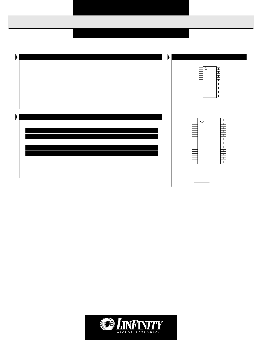
DP PACKAGE:
THERMAL RESISTANCE-JUNCTION TO LEADS,
JL
20∞C/W
THERMAL RESISTANCE-JUNCTION TO AMBIENT,
JA
50∞C/W
PWP PACKAGE:
THERMAL RESISTANCE-JUNCTION TO LEADS,
JL
27∞C/W
THERMAL RESISTANCE-JUNCTION TO AMBIENT,
JA
100∞C/W
Junction Temperature Calculation: T
J
= T
A
+ (P
D
x
JA
).
The
JA
numbers are guidelines for the thermal performance of the device/pc-board
system. All of the above assume no ambient airflow.
THERMAL DATA
ABSOLUTE MAXIMUM RATINGS
(Note 1)
PACKAGE PIN OUTS
PWP PACKAGE
(Top View)
T6
T5
N.C.
N.C.
HEATSINK/GND
HEATSINK/GND
HEATSINK/GND
HEATSINK/GND
N.C.
V
TERM
T4
T3
1
24
2
23
3
22
4
21
5
20
6
19
7
18
8
17
9
16
10
15
11
14
12
13
T7
T8
T9
N.C.
GND
HEATSINK/GND
HEATSINK/GND
HEATSINK/GND
HEATSINK/GND
DISCONNECT *
T1
T2
T7
T8
T9
HEATSINK/GND
GND
DISCONNECT *
T1
T2
T6
T5
N.C.
HEATSINK/GND
HEATSINK/GND
V
TERM
T4
T3
1
16
2
15
3
14
4
13
5
12
6
11
7
10
8
9
DP PACKAGE
(Top View)
*
Pin 10 is DISCONNECT for the LX5112A,
and DISCONNECT for the LX5111A.
U L T R A 9 - C
H A N N E L
S C S I T
E R M I N A T O R
LX5111A/5112A
P R O D U C T D A T A B O O K 1 9 9 6 / 1 9 9 7
3
Copyright © 1999
Rev. 0.1 3/99
P
R E L I M I N A R Y
D
A T A
S
H E E T
UltraMAX
2.65
2.82
V
2.1
2.2
V
5
9
mA
205
225
mA
275
µA
275
µA
-21
-23
-24
mA
-17
-18
mA
10
nA
40
µA
-14
µA
10
nA
10
nA
10
nA
3
pF
35
MHz
7
11
mA
Termination Voltage
V
TERM
High Level Enable Input Voltage
LX5111A
V
IH
LX5112A
Low Level Disable Input Voltage
LX5111A
V
IL
LX5112A
Operating Virtual Junction Temperature Range
LX5111AC/5112AC
R E C O M M E N D E D O P E R AT I N G C O N D I T I O N S
(Note 2)
Parameter
Symbol
Units
Recommended Operating Conditions
Min.
Typ.
Max.
3.0
5.5
V
2.5
V
TERM
V
0
0.8
V
0
0.8
V
2.5
V
TERM
V
0
125
∞C
Note 2. Range over which the device is functional.
E L E C T R I C A L C H A R A C T E R I S T I C S
Term Power = 4.75V unless otherwise specified. Unless otherwise specified, these specifications apply at the recommended operating ambient tempera-
ture of T
A
= 25∞C. Low duty cycle pulse testing techniques are used which maintains junction and case temperatures equal to the ambient temperature.
Parameter
Symbol
Test Conditions
Units
LX5111A/5112A
Min.
Typ.
Max.
Output High Voltage
V
OUT
Term Power = 4.75V
Term Power = 3.0V
TermPwr Supply Current
I
CC
All data lines = open
All data lines = 0.5V
LX5111A
DISCONNECT Pin < 0.8V
LX5112A
DISCONNECT Pin > 2.0V
Output Current
I
OUT
V
OUT
= 0.5V, Term Power = 4.75V
V
OUT
= 0.5V, Term Power = 3.0V
DISCONNECT Input Current
LX5111A
I
IN
DISCONNECT Pin = 4.75V
DISCONNECT Pin = 0V
DISCONNECT Input Current
LX5112A
I
IN
DISCONNECT Pin = 0V
DISCONNECT Pin = 4.75V
Output Leakage Current
LX5111A
I
OL
DISCONNECT Pin = < 0.8V, V
O
= 0.5V
LX5112A
DISCONNECT Pin = > 2.0V, V
O
= 0.5V
Capacitance in DISCONNECT Mode
C
OUT
V
OUT
= 0V, frequency = 1MHz
Channel Bandwidth
BW
Termination Sink Current, per Channel
I
SINK
V
OUT
= 4V
U L T R A 9 - C
H A N N E L
S C S I T
E R M I N A T O R
LX5111A/5112A
P R O D U C T D A T A B O O K 1 9 9 6 / 1 9 9 7
Copyright © 1999
Rev. 0.1 3/99
4
P
R E L I M I N A R Y
D
A T A
S
H E E T
UltraMAX
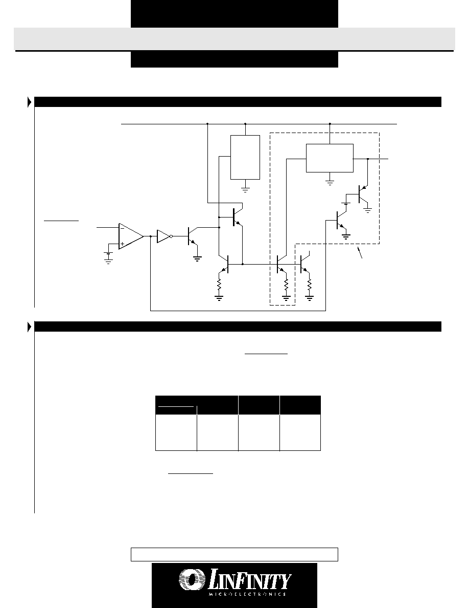
B L O C K D I A G R A M
F U N C T I O N A L D E S C R I P T I O N
TERM POWER
CURRENT
BIASING
CIRCUIT
1.4V
DISCONNECT (5111)
DISCONNECT (5112)
24mA CURRENT
LIMITING CIRCUIT
DATA OUTPUT
PIN DB(0)
2.85V
1 OF 9 CHANNELS
Cable transmission theory suggests to optimize signal speed
and quality, the termination should act both as an ideal voltage
reference when the line is released (deasserted) and as an ideal
current source when the line is active (asserted). Common
active terminators, which consist of Linear Regulators in series
with resistors (typically 110
), are
a compromise. As the line voltage
increases, the amount of current
decreases linearly by the equation
V = I * R. The LX5111A/5112A, with
their unique new architecture ap-
plies the maximum amount of
current regardless of line voltage
until the termination high threshold
(2.85V) is reached.
Acting as a near ideal line terminators, the LX5111A/5112A
closely reproduce the optimum case when the devices are
enabled. To enable the device the DISCONNECT pin
(DISCONNECT pin for the LX5112A) must be pulled logic High
(logic Low for the LX5112A). During this mode of operation,
quiescent current is 6mA and the devices will respond to line
demands by delivering 24mA on assertion, and by imposing
2.85V on deassertion. In order to disable the device, the
DISCONNECT pin (DISCONNECT pin for the LX5112A) must
be driven logic Low (logic High for the LX5112A). This mode
of operation places the devices in a sleep state where a meager
275µA of quiescent current is con-
sumed. Additionally, all outputs are
in a Hi-Z (impedance) state. Sleep
mode can be used for power con-
servation or to completely eliminate
the terminator from the SCSI chain.
In the second case, termination
node capacitance is important to
consider. The terminators will ap-
pear as a parasitic distributed capaci-
tance on the line, which can detract from bus performance. For
this reason, the LX5111A/5112A have been optimized to have
only 3pF of capacitance per output in the sleep state.
An additional feature of the LX5111A/5112A IC's are their
compatibility with active negation drivers.
UltraMAX is a trademark of Linfinity Microelectronics Inc.
Outputs
Quiescent
Current
H
L
Enabled
6mA
L
H
HI Z
275µA
Open
Open
HI Z
275µA
LX5111A
LX5112A
DISCONNECT
DISCONNECT
P
OWER
U
P
/ P
OWER
D
OWN
F
UNCTION
T
ABLE
PRELIMINARY DATA - Information contained in this document is pre-production data, and is proprietary to LinFinity. It may
not modified in any way without the express written consent of LinFinity. Product referred to herein is offered in sample form
only, and Linfinity reserves the right to change or discontinue this proposed product at any time.