 | ÐлекÑÑоннÑй компоненÑ: LX5510-LQ | СкаÑаÑÑ:  PDF PDF  ZIP ZIP |
Äîêóìåíòàöèÿ è îïèñàíèÿ www.docs.chipfind.ru
LX5510
P
RELIMINARY
D
ATA
S
HEET
C
C
O
O
N
N
F
F
I
I
D
D
E
E
N
N
T
T
I
I
A
A
L
L
Microsemi
Integrated Products Division
11861 Western Avenue, Garden Grove, CA. 92841, 714-898-8121, Fax: 714-893-2570
Page 1
Copyright
2003
Rev. 0.3g, 2003-05-08
WWW
.
Microse
m
i
.
CO
M
InGaP HBT 2.4 2.5 GHz Power Amplifier
I N T E G R A T E D P R O D U C T S
D E S C R I P T I O N
The LX5510 is a power amplifier
optimized for WLAN applications in
the 2.4-2.5GHz frequency range. The
PA is implemented as a two-stage
monolithic microwave integrated
circuit (MMIC) with active bias and
input/output pre-matching.
The device is manufactured with an
InGaP/GaAs Heterojunction Bipolar
Transistor (HBT) IC process
(MOCVD). With single low voltage
supply of 3.3V 20dB power gain
between 2.4-2.5GHz, at a low
quiescent current of 65mA.
For +19dBm OFDM output power
(64QAM, 54Mbps), the PA provides a
low EVM (Error-Vector Magnitude) of
3.0%, and consumes 120mA total DC
current with the nominal 3.3V bias.
With increased bias of 4.5V EVM is ~
5% at 23dBm.
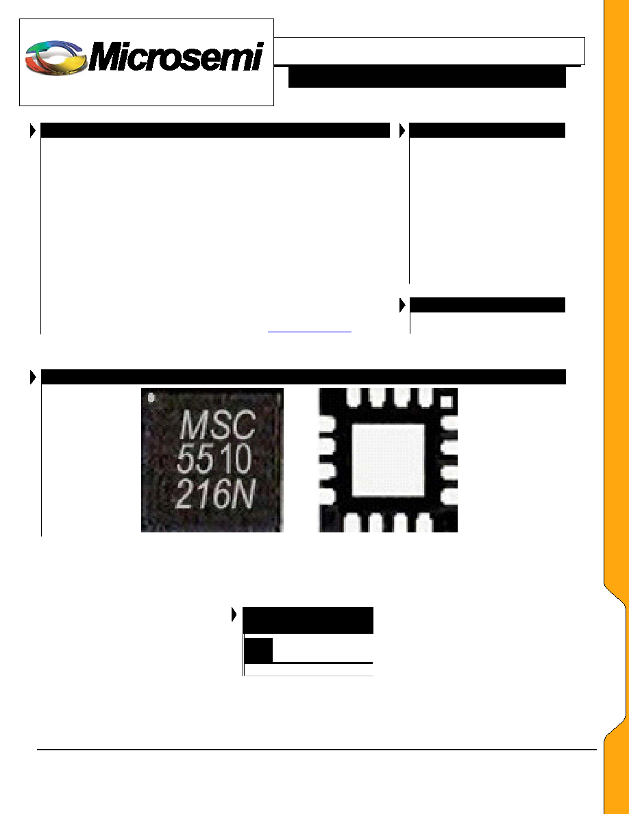
The LX5510 is available in a 16-pin
3mmx3mm micro-lead package (MLP).
The compact footprint, low profile, and
excellent thermal capability of the MLP
package makes the LX5510 an ideal
solution for medium-gain power
amplifier requirements for IEEE
802.11b/g applications
IMPORTANT: For the most current data, consult MICROSEMI's website:
http://www.microsemi.com
K E Y F E A T U R E S
Advanced InGaP HBT
2.4 2.5GHz Operation
Single-Polarity 3.3V Supply
Low Quiescent Current Icq
~65mA
Power Gain ~20dB @ 2.45GHz
and Pout = 19dBm
Total Current 120mA for Pout =
19dBm @ 2.45GHz OFDM
EVM ~ 3.0% for 64QAM /
54Mbps and Pout = 19dBm
Small Footprint (3x3mm
2
)
Low Profile (0.9mm)
A P P L I C A T I O N S
IEEE 802.11b/g
P R O D U C T H I G H L I G H T
P A C K A G E O R D E R
I N F O
LQ
Plastic MLPQ
16 pin
LX5510-LQ
Note: Available in Tape & Reel.
Append the letter "T" to the part number.
(i.e. LX5510-LQT)
L
L
X
X
5
5
5
5
1
1
0
0

LX5510
P
RELIMINARY
D
ATA
S
HEET
C
C
O
O
N
N
F
F
I
I
D
D
E
E
N
N
T
T
I
I
A
A
L
L
Microsemi
Integrated Products Division
11861 Western Avenue, Garden Grove, CA. 92841, 714-898-8121, Fax: 714-893-2570
Page 2
Copyright
2003
Rev. 0.3g, 2003-05-08
WWW
.
Microse
m
i
.
CO
M
InGaP HBT 2.4 2.5 GHz Power Amplifier
I N T E G R A T E D P R O D U C T S
A B S O L U T E M A X I M U M R A T I N G S
DC Supply Voltage, RF off ...............................................................................6V
Collector Current ........................................................................................400mA
Total Power Dissipation....................................................................................2W
RF Input Power........................................................................................... 15dBm
Maximum Junction Temperature (T
J
max) .................................................. 150°C
Operation Ambient Temperature ...................................................-40°C to +85°C
Storage Temperature....................................................................-60°C to +150°C
Note: Exceeding these ratings could cause damage to the device. All voltages are with respect to
Ground. Currents are positive into, negative out of specified terminal
.
x denotes
respective pin designator 1, 2, or 3
P A C K A G E P I N O U T
RF IN
RF IN
VB1
VB
2
VC
C
RF OUT
RF OUT
VC
1
VC2
*
1
2
3
4
5
6
7
8
9
10
11
12
13 14 15 16
* Pad is Ground
GND
GND
GND
GND
GND
GN
D
GN
D
LQ
P
ACKAGE
(Bottom View)
F U N C T I O N A L P I N D E S C R I P T I O N
Name Description
RF IN
RF input for the power amplifier. This pin is DC-shorted to GND but AC-coupled to the transistor base of the first
stage.
VB1
Bias current control voltage for the first stage.
VB2
Bias current control voltage for the second stage. The VB2 pin can be connected with the first stage control
voltage (VB1) into a single reference voltage (referred to as Vref) through an external resistor bridge.
VCC
Supply voltage for the bias reference and control circuits. This pin can be combined with both VC1 and VC2
pins, resulting in a single supply voltage (referred to as Vc).
RF OUT
RF output for the power amplifier.
VC1
Power supply for first stage amplifier. The VC1 feedline should be terminated with a 4pF bypass capacitor 50mil
apart from the device, followed by a 8.2nH blocking inductor at the supply side. This pin can be combined with
VC2 and VCC pins, resulting in a single supply voltage (referred to as Vc).
VC2
Power supply for second stage amplifier. The VC2 feedline should be driven with a 8.2nH AC blocking inductor
and 1uF bypass capacitor. This pin can be combined with VC1 and VCC pins, resulting in a single supply
voltage (referred to as Vc).
GND
The center metal base of the MLP package provides both DC and RF ground as well as heat sink for the power
amplifier.
P
P
A
A
C
C
K
K
A
A
G
G
E
E
D
D
A
A
T
T
A
A

LX5510
P
RELIMINARY
D
ATA
S
HEET
C
C
O
O
N
N
F
F
I
I
D
D
E
E
N
N
T
T
I
I
A
A
L
L
Microsemi
Integrated Products Division
11861 Western Avenue, Garden Grove, CA. 92841, 714-898-8121, Fax: 714-893-2570
Page 3
Copyright
2003
Rev. 0.3g, 2003-05-08
WWW
.
Microse
m
i
.
CO
M
InGaP HBT 2.4 2.5 GHz Power Amplifier
I N T E G R A T E D P R O D U C T S
E L E C T R I C A L C H A R A C T E R I S T I C S
Unless otherwise specified, the following specifications apply over the operating ambient temperature 0
°C
T
A
70
°C except where
otherwise noted and the following test conditions: Vc = 3.3V, Vref = 2.85V, Icq = 65mA, T
A
= 25°C
LX5510
Parameter Symbol
Test
Conditions
Min Typ Max
Units
Frequency
Range
f
2.4
2.5 GHz
Power Gain at Pout = 19dBm
Gp
20
dB
EVM at Pout = 19dBm
64QAM / 54Mbps
3.0
%
Total Current at Pout = 19dBm
Ictotal
120
mA
Quiescent
Current
Icq
65
mA
Bias Control Reference Current
Iref
For Icq = 65mA
1.2
mA
Small-Signal
Gain
S21
20
dB
Gain
Flatness
S21 Over
100MHz
±0.5
dB
Gain Variation Over
Temperature
S21
-40°C to +85°C
TBD
dB
Input
Return
Loss
S11
10
dB
Output
Return
Loss
S22
10
dB
Reverse
Isolation
S12
-40
dB
Second Harmonic
Pout = 19dBm
-60
dBc
Third Harmonic
Pout = 19dbm
-50
dBc
Noise
Figure
NF
TBD
dB
Ramp-On
Time
t
ON
10 ~ 90%
100
ns
Note: All measured data was obtained on a 10mil GETEK evaluation board without heat sink.
E
E
L
L
E
E
C
C
T
T
R
R
I
I
C
C
A
A
L
L
S
S
LX5510
P
RELIMINARY
D
ATA
S
HEET
C
C
O
O
N
N
F
F
I
I
D
D
E
E
N
N
T
T
I
I
A
A
L
L
Microsemi
Integrated Products Division
11861 Western Avenue, Garden Grove, CA. 92841, 714-898-8121, Fax: 714-893-2570
Page 4
Copyright
2003
Rev. 0.3g, 2003-05-08
WWW
.
Microse
m
i
.
CO
M
InGaP HBT 2.4 2.5 GHz Power Amplifier
I N T E G R A T E D P R O D U C T S
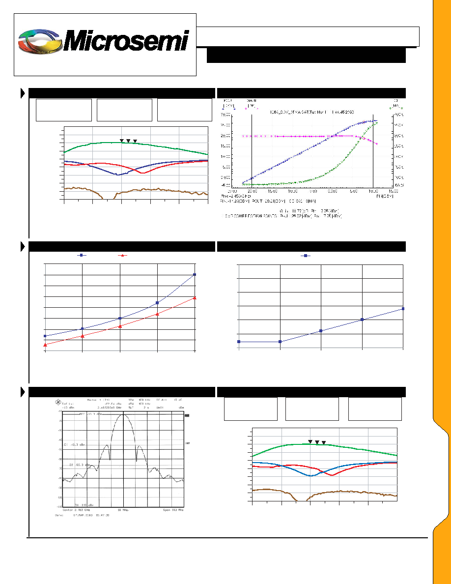
S P A R A M E T E R ( 3 . 3 V )
P O W E R S W E E P
m1
freq=2.400GHz
dB(S (2,1))=19.788
m2
freq=2.450GHz
dB(S (2,1))=19.421
m7
freq=2.500GHz
dB(S (2,1))=18.846
2.2
2.4
2.6
2.8
2.0
3.0
-40
-30
-20
-10
0
10
20
30
-50
40
Frequency GHz
dB
(
S
(
1,1)
)
dB
(
S
(
1,2)
)
dB
(
S
(
2,1)
)
m1
m2
m7
dB
(
S
(
2,2)
)
Figure 1 S-Parameter Data
(VC = 3.3V, VREF = 2.85V, Icq = 65mA)
Figure 2 Power Sweep
(Vc = 3.3V, Vref = 2.85V, Icq = 65mA)
E V M D A T A
A C P D A T A
0
1
2
3
4
5
6
7
8
17
18
19
20
21
Output Power (dBm)
E
V
M
(%)
100
110
120
130
140
150
160
170
180
C
u
rre
nt
(m
A)
EVM_PA_ONLY
CURRENT_3.3V
Figure 3 EVM Data with 54Mbps 64QAM OFDM
(Vc = 3.3V, Vref = 2.85V, Icq = 65mA, Frequency = 2.45GHz)
-55
-52.5
-50
-47.5
-45
-42.5
-40
17
18
19
20
21
Output Power (dBm)
ACP
(
d
Bc
)
ACP_30MHz
Figure 4 ACP Data with 54Mbps 64QAM OFDM
(VC = 3.3V, Vref = 2.85V, Icq = 65mA, Frequency = 2.45GHz)
C C K S P E C T R U M
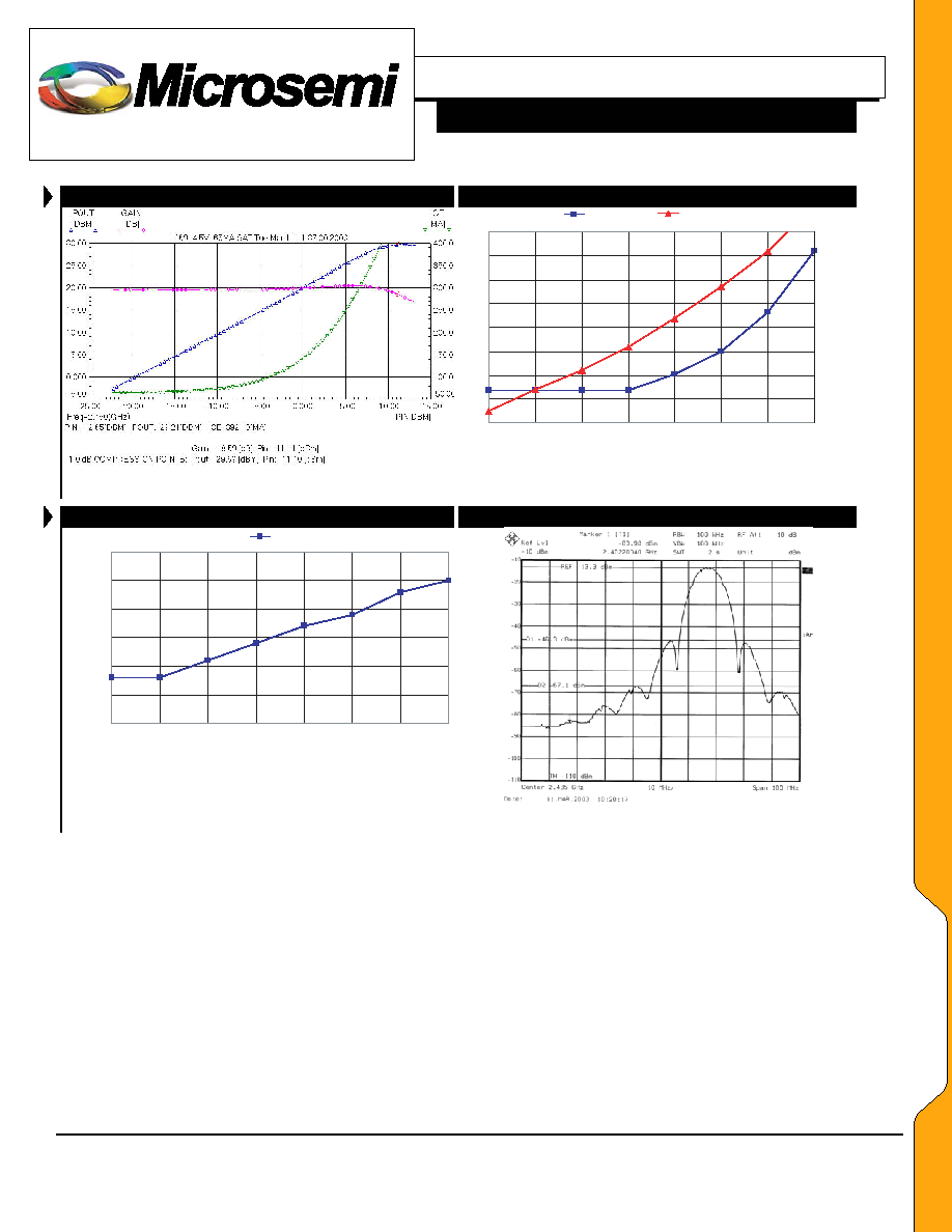
S P A R A M E T E R ( 4 . 5 V )
Figure 5 Spectrum with 23dBm 11Mb/s CCK
(Vc = 3.3V, Vref =2.85V, Icq = 65mA, Ic = 180mA, Freq = 2.45GHz)
m1
freq=2.400GHz
S21 (dB)=20.041
m2
freq=2.450GHz
S21 (dB)=19.710
m7
freq=2.500GHz
S21 (dB)=19.143
2.2
2.4
2.6
2.8
2.0
3.0
-40
-30
-20
-10
0
10
20
30
-50
40
frequency (GHz)
dB
(
S
(
1,1)
)
dB
(
S
(
1,2)
)
dB
(
S
(
2,1)
)
m1
m2
m7
dB
(
S
(
2,2)
)
Figure 6 S-Parameter Data
(Vc = 4.5V, Vref = 2.85V, Icq = 65mA)
G
G
R
R
A
A
P
P
H
H
S
S
LX5510
P
RELIMINARY
D
ATA
S
HEET
C
C
O
O
N
N
F
F
I
I
D
D
E
E
N
N
T
T
I
I
A
A
L
L
Microsemi
Integrated Products Division
11861 Western Avenue, Garden Grove, CA. 92841, 714-898-8121, Fax: 714-893-2570
Page 5
Copyright
2003
Rev. 0.3g, 2003-05-08
WWW
.
Microse
m
i
.
CO
M
InGaP HBT 2.4 2.5 GHz Power Amplifier
I N T E G R A T E D P R O D U C T S
P O W E R S W E E P
E V M D A T A
Figure 7 Power Sweep
(Vc = 4.5V, Vref = 2.85V, Icq = 65mA)
0
1
2
3
4
5
6
7
8
17
18
19
20
21
22
23
24
Output Power (dBm)
EVM (%)
100
110
120
130
140
150
160
170
180
Current (mA)
EVM_PA_ONLY
CURRENT_4.5V
Figure 8 EVM Data with 54Mbps 64QAM OFDM
(Vc = 4.5V, Vref = 2.85V, Icq =65mA, Frequency =2.45GHz)
A C P D A T A
C C K S P E C T R U M
-60
-57.5
-55
-52.5
-50
-47.5
-45
17
18
19
20
21
22
23
24
Output Power (dBm)
ACP
(dBc)
ACP_30MHz
Figure 9 ACP Data with 54Mbps 64QAM OFDM
(Vc = 4.5V, Vref = 2.85V, Icq = 65mA, Frequency = 2.45GHz)
Figure 10 Spectrum with 23dBm 11Mb/s CCK
(Vc = 4.5V, Vref = 2.85V, Icq = 65mA, Ic = 180mA, Freq = 2.45GHz)
G
G
R
R
A
A
P
P
H
H
S
S