LX8415-25
2.5V
LX8415-33
3.3V
LX8415-00
Adjustable
LIN D
O C
#: 8415
Note: All surface-mount packages are available in Tape & Reel.
Append the letter "T" to part number (i.e. LX8415-33CSTT).
"xx" refers to output voltage, please see table above.
D E S C R I P T I O N
K E Y F E A T U R E S
s 0.7% Line Regulation Maximum
s 0.7% Load Regulation Maximum
s Output Current Of 500mA
s Regulates To <1.3V Dropout
s Space Saving SOT-223 Surface
Mount Package
s Guaranteed Dropout Voltage At Multiple
Current Levels
s 3-Terminal Adjustable, Fixed 2.5V And
Fixed 3.3V
The LX8415 series ICs are positive Low
Dropout (LDO) regulators. At the de-
signed maximum load current, the
LX8415 series dropout voltage is guar-
anteed to be 1.3V or lower at 0.5A. The
dropout voltage decreases with load
current.
The LX8415 is available in an adjust-
able output voltage version and fixed
output versions of 2.5V and 3.3V. On-
chip trimming of the internal voltage
reference allows specification of the
initial output voltage to within �1% of
its nominal value. The output current-
limit point is also trimmed, which helps
to minimize stress on both the regulator
and the system power source when they
are operated under short-circuit condi-
tions. The regulator's internal circuitry
will operate at input-to-output differen-
tial voltages down to 1V.
Most regulator circuit designs include
output capacitors with values in the
range of tens to hundreds of microfarads
or more. The LX8415 typically requires
at least 10�F of output capacitance for
stable operation.
The LX8415 is available in the low-
profile plastic SOT-223 package for ap-
plications where space is at a premium.
P R O D U C T H I G H L I G H T
L
OW
C
OST
5V
TO
3.3V R
EGULATOR
0 . 5 A L
O W
D
R O P O U T
P
O S I T I V E
R
E G U L A T O R S
P
R E L I M I N A R Y
D
A T A
S
H E E T
T
H E
I
N F I N I T E
P
O W E R
O F
I
N N O V A T I O N
LX8415-xx
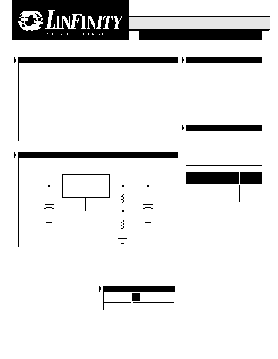
A P P L I C A T I O N S
s Battery Chargers
s 5V To 3.3V Linear Regulators
s Post Regulators For Switching Supplies
s Modems
s DVD Players
PA C K A G E O R D E R I N F O
T
A
(�C)
Plastic SOT-223
3-pin
ST
0 to 125
LX8415-xxCST
Part #
Output
Voltage
A
VA I L A B L E
O
P T I O N S
P E R
P
A RT
#
Copyright � 1999
Rev. 0.4 1/99
1
11861 W
ESTERN
A
VENUE
, G
ARDEN
G
ROVE
, CA. 92841, 714-898-8121, F
AX
: 714-893-2570
L
I N
F
I N I T Y
M
I C R O E L E C T R O N I C S
I
N C
.
LX8415-xx
OUT
IN
ADJ
V
OUT
3.3V
V
IN
5V
R
1
60.4
R
2
100
10�F
22�F
NOTE: For current data & package dimensions, visit our web site: http://www.linfinity.com.
0 . 5 A L
O W
D
R O P O U T
P
O S I T I V E
R
E G U L A T O R S
LX8415-xx
P R O D U C T D A T A B O O K 1 9 9 6 / 1 9 9 7
Copyright � 1999
Rev. 0.4 1/99
2
P
R E L I M I N A R Y
D
A T A
S
H E E T
ABSOLUTE MAXIMUM RATINGS
(Note 1)
Power Dissipation .................................................................................. Internally Limited
Input Voltage
LX8415-00 (Adjustable) / 8415-33 (3.3V) .................................................................. 7V
Surge Voltage ................................................................................................................. 7V
Operating Junction Temperature
Plastic (ST, DD & DT Packages) .......................................................................... 150�C
Storage Temperature Range ...................................................................... -65�C to 150�C
Lead Temperature (Soldering, 10 seconds) ............................................................. 300�C
Short-Circuit Protection ....................................................................................... Indefinite
Note 1. Exceeding these ratings could cause damage to the device. All voltages are with
respect to Ground. Currents are positive into, negative out of the specified terminal.
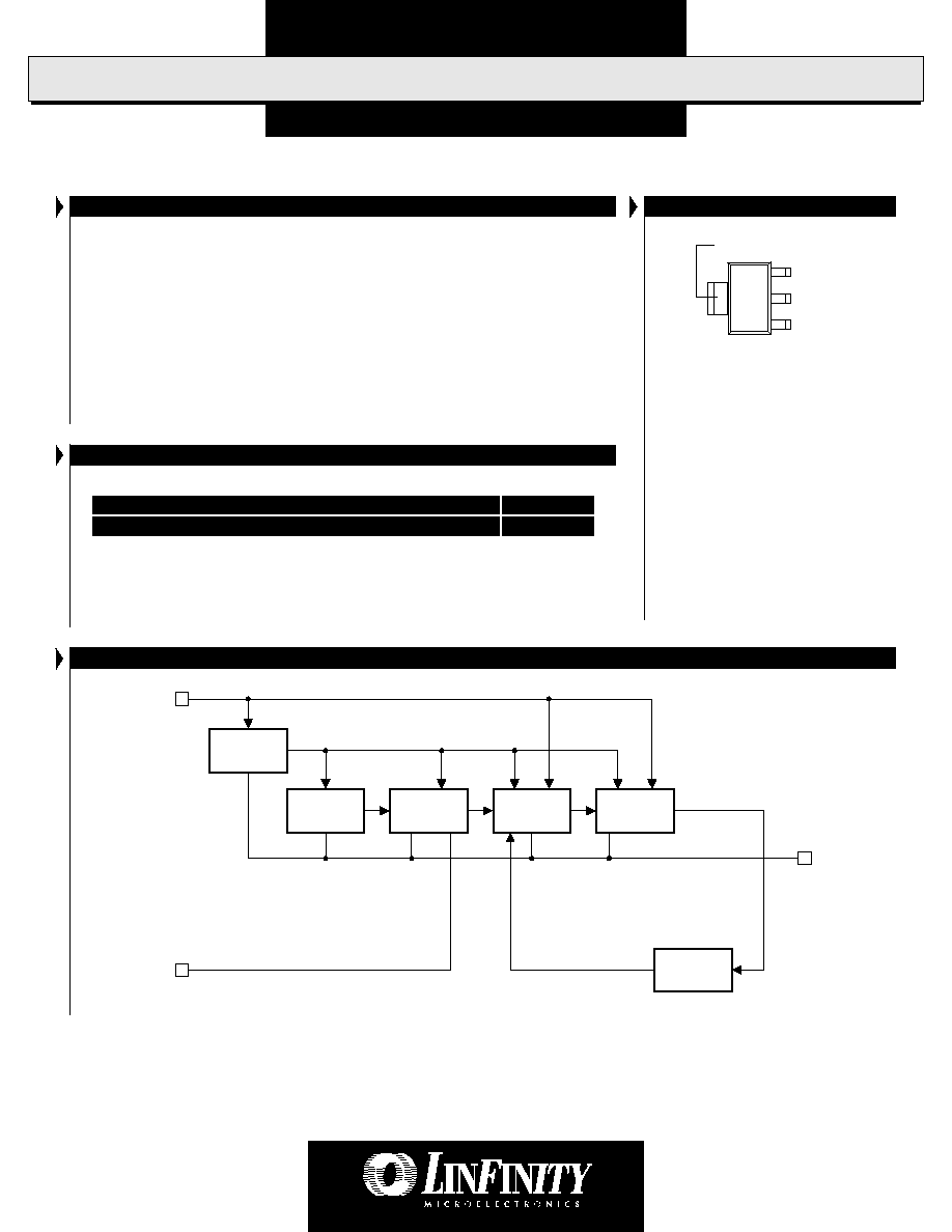
PACKAGE PIN OUTS
3. IN
2. OUT
1. ADJ / GND
ST PACKAGE
(Top View)
THERMAL DATA
ST PACKAGE:
THERMAL RESISTANCE-JUNCTION TO TAB,
JT
15�C/W
THERMAL RESISTANCE-JUNCTION TO AMBIENT,
JA
*150�C/W
Junction Temperature Calculation: T
J
= T
A
+ (P
D
x
JA
). The
JA
numbers are guidelines for the
thermal performance of the device/pc-board system. All of the above assume no ambient airflow.
*
JA
can be improved with package soldered to 0.5IN
2
copper area over backside ground
plane or internal power plane.
JA
can vary from 20�C/W to > 40�C/W depending on
mounting technique. (See Application Notes Section: Thermal Considerations)
TAB IS V
OUT
BLOCK DIAGRAM
Thermal
Limit Circuit
Control
Circuit
Bandgap
Circuit
Output
Circuit
Bias
Circuit
V
OUT
V
IN
Current
Limit Circuit
ADJ
0 . 5 A L
O W
D
R O P O U T
P
O S I T I V E
R
E G U L A T O R S
LX8415-xx
P R O D U C T D A T A B O O K 1 9 9 6 / 1 9 9 7
3
Copyright � 1999
Rev. 0.4 1/99
P
R E L I M I N A R Y
D
A T A
S
H E E T
Input Voltage
Operating Voltage
LX8415-xx
Operating Ambient Temperature Range
R E C O M M E N D E D O P E R AT I N G C O N D I T I O N S
(Note 2)
Parameter
Symbol
Units
Recommended Operating Conditions
Min.
Typ.
Max.
7
V
0
125
�C
Note 2. Range over which the device is functional.
1.238
1.250
1.262
V
1.225
1.250
1.275
V
2.475
2.500
2.525
V
2.450
2.500
2.550
V
3.267
3.300
3.333
V
3.235
3.300
3.365
V
0.05
0.7
%
1
7
mV
0.15
0.5
%
10
20
mV
1.05
1.20
V
1.10
1.25
V
1.15
1.30
V
500
950
mA
0.5
10
mA
4.5
10
mA
0.08
0.2
%/W
60
75
dB
60
130
�A
0.2
5
�A
0.5
%
0.3
%
0.003
%
E L E C T R I C A L C H A R A C T E R I S T I C S
(Unless otherwise specified: 0�C
T
J
125�C, I
MAX
= 0.5A for the LX8415-xx.)
Parameter
Symbol
Test Conditions
Units
LX8415-xx
Min.
Typ.
Max.
Reference Voltage
LX8415-00
V
REF
I
OUT
= 10mA, (V
IN
- V
OUT
) = 2V, T
J
= 25�C
10mA
I
OUT
I
MAX
, 1.5V
(V
IN
- V
OUT
)
6V
Output Voltage
LX8415-25
I
OUT
= 10mA, V
IN
= 5V, T
J
= 25�C
0mA
I
OUT
I
MAX
, 4.75V
V
IN
6V
LX8415-33
I
OUT
= 10mA, V
IN
= 5V, T
J
= 25�C
0mA
I
OUT
I
MAX
, 4.75V
V
IN
6V
Line Regulation
LX8415-00
I
OUT
= 10mA, 1.5V
V
IN
- V
OUT
6V
(Note 3)
LX8415-25 / 33
I
OUT
= 0mA, 4.75V
V
IN
6V
Load Regulation
LX8415-00
(V
IN
- V
OUT
) = 3V, 10mA
I
OUT
I
MAX
(Note 3)
LX8415-25 / 33
V
IN
= 4.75V, 0mA
I
OUT
I
MAX
Dropout Voltage
LX8415-xx
I
OUT
= 100mA
(Note 4)
I
OUT
= 300mA
I
OUT
= I
MAX
Current Limit
LX8415-xx
I
OUT (MAX)
(V
IN
- V
OUT
)
1.3V, T
J
= 25�C
Minimum Load Current (Note 5)
V
IN
6V, (LX8415-00)
Quiescent Current
LX8415-25 / 33
V
IN
6V
Thermal Regulation
T
A
= 25�C, 30ms Pulse
Ripple Rejection
f
RIPPLE
= 120Hz, (V
IN
- V
OUT
) = 3V, V
RIPPLE
= 1Vp - p
Adjust Pin Current
LX8415(A)-00
Adjust Pin Current Change LX8415(A)-00
10mA
I
OUT
I
MAX
, 1.5V
(V
IN
- V
OUT
)
6V
Temperature Stability
Long Term Stability
T
A
= 125�C, 1000Hrs
RMS Output Noise
(% of V
OUT
), 10Hz
f
10kHz
Notes: 3. See thermal regulation specification for changes in output voltage due to heating effects. Load regulation and line regulation are measured at a constant junction
temperature by low duty cycle pulse testing.
4. Dropout voltage is specified over the full output current range of the device. Dropout voltage is defined as the minimum input/output differential measured at the
specified output current. Test points and limits are also shown on the Dropout Voltage Curve.
5. Minimum load current is defined as the minimum output current required to maintain regulation.
0 . 5 A L
O W
D
R O P O U T
P
O S I T I V E
R
E G U L A T O R S
LX8415-xx
P R O D U C T D A T A B O O K 1 9 9 6 / 1 9 9 7
Copyright � 1999
Rev. 0.4 1/99
4
P
R E L I M I N A R Y
D
A T A
S
H E E T
A P P L I C A T I O N N O T E S
The LX8415 series ICs are easy to use Low-Dropout (LDO) voltage
regulators. They have the standard self-protection features ex-
pected of a voltage regulator: short circuit protection and automatic
thermal shutdown if the device temperature rises above approxi-
mately 165�C.
Use of an output capacitor is REQUIRED with the LX8415 series.
Please see the table below for recommended minimum capacitor
values.
These regulators offer a more tightly controlled reference voltage
tolerance and superior reference stability when measured against
the older pin-compatible regulator types that they replace.
STABILITY
The output capacitor is part of the regulator's frequency compen-
sation system. Many types of capacitors are available, with different
capacitance value tolerances, capacitance temperature coefficients,
and equivalent series impedances. For all operating conditions,
connection of a 220�F aluminum electrolytic capacitor or a 47�F
solid tantalum capacitor between the output terminal and ground
will guarantee stable operation.
If a bypass capacitor is connected between the output voltage
adjust (ADJ) pin and ground, ripple rejection will be improved
(please see the section entitled "RIPPLE REJECTION"). When ADJ
pin bypassing is used, the required output capacitor value increases.
Output capacitor values of 220�F (aluminum) or 47�F (tantalum)
provide for all cases of bypassing the ADJ pin. If an ADJ pin bypass
capacitor is not used, smaller output capacitor values are adequate.
The table below shows recommended minimum capacitance values
for stable operation.
INPUT
OUTPUT
ADJ
10�F
15�F Tantalum, 100�F Aluminum
None
10�F
47�F Tantalum, 220�F Aluminum
15�F
In order to ensure good transient response from the power supply
system under rapidly changing current load conditions, designers
generally use several output capacitors connected in parallel. Such
an arrangement serves to minimize the effects of the parasitic
resistance (ESR) and inductance (ESL) that are present in all
capacitors. Cost-effective solutions that sufficiently limit ESR and
ESL effects generally result in total capacitance values in the range
of hundreds to thousands of microfarads, which is more than
adequate to meet regulator output capacitor specifications. Output
capacitance values may be increased without limit.
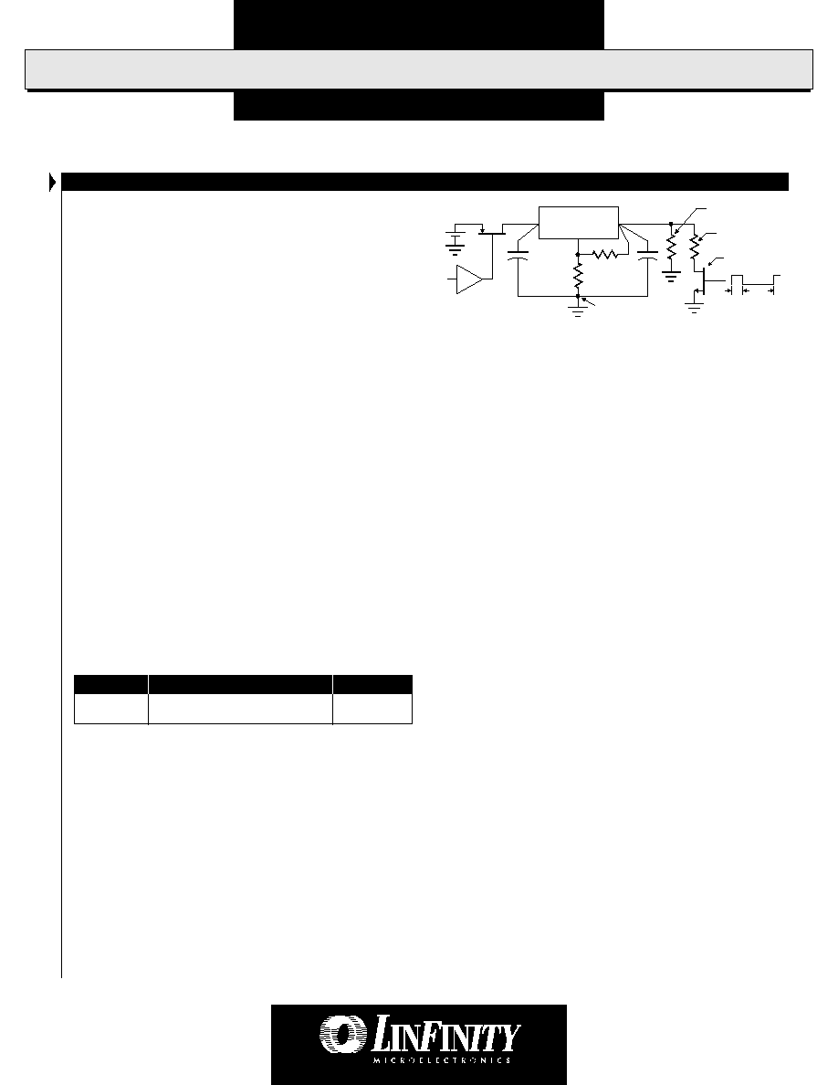
The circuit shown in Figure 1 can be used to observe the transient
response characteristics of the regulator in a power system under
changing loads. The effects of different capacitor types and values
on transient response parameters, such as overshoot and under-
shoot, can be quickly compared in order to develop an optimum
solution.
RECOMMENDED CAPACITOR VALUES
FIGURE 1 -- DYNAMIC INPUT and OUTPUT TEST
LX8415-xx
Power Supply
OUT
IN
ADJ
Star Ground
1 sec
10ms
R
DSON
<< R
L
Full Load
(Smaller resistor)
Minumum Load
(Larger resistor)
C
1
C
2
RIPPLE REJECTION
Ripple rejection can be improved by connecting a capacitor
between the ADJ pin and ground. The value of the capacitor should
be chosen so that the impedance of the capacitor is equal in
magnitude to the resistance of R1 at the ripple frequency. The
capacitor value can be determined by using this equation:
C = 1 / (6.28 * F
R
* R1)
where: C
the value of the capacitor in Farads;
select an equal or larger standard value.
F
R
the ripple frequency in Hz
R1
the value of resistor R1 in ohms
At a ripple frequency of 120Hz, with R1 = 100
:
C = 1 / (6.28 * 120Hz * 100
) = 13.3�F
The closest equal or larger standard value should be used, in this
case, 15�F.
When an ADJ pin bypass capacitor is used, output ripple
amplitude will be essentially independent of the output voltage. If
an ADJ pin bypass capacitor is not used, output ripple will be
proportional to the ratio of the output voltage to the reference
voltage:
M = V
OUT
/V
REF
where: M
a multiplier for the ripple seen when the
ADJ pin is optimally bypassed.
V
REF
= 1.25V.
For example, if V
OUT
= 2.5V the output ripple will be:
M = 2.5V/1.25V= 2
Output ripple will be twice as bad as it would be if the ADJ pin
were to be bypassed to ground with a properly selected capacitor.
0 . 5 A L
O W
D
R O P O U T
P
O S I T I V E
R
E G U L A T O R S
LX8415-xx
P R O D U C T D A T A B O O K 1 9 9 6 / 1 9 9 7
5
Copyright � 1999
Rev. 0.4 1/99
P
R E L I M I N A R Y
D
A T A
S
H E E T
A P P L I C A T I O N N O T E S
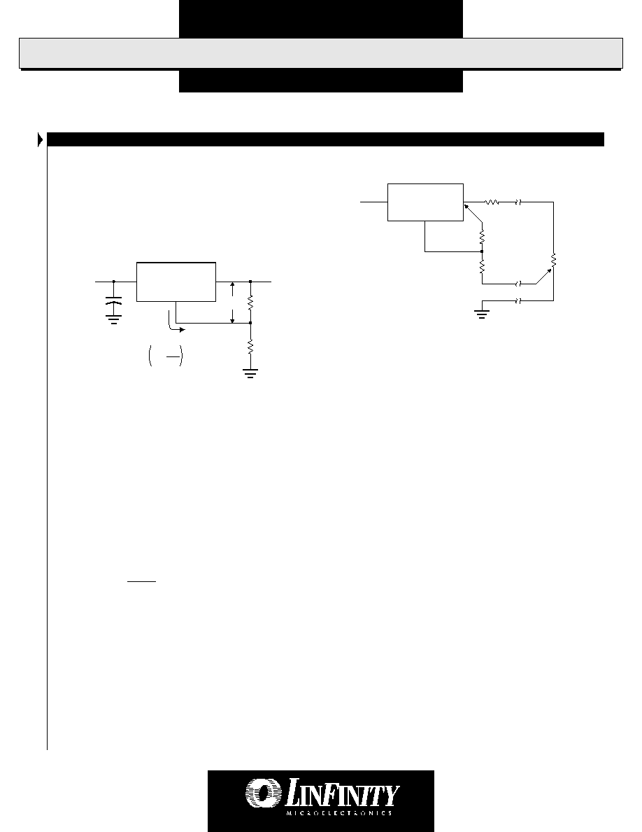
FIGURE 2 -- BASIC ADJUSTABLE REGULATOR
R2+R1
R1
LX8415-xx
OUT
IN
ADJ
V
OUT
V
IN
R1
R2
V
REF
I
ADJ
50�A
V
OUT
= V
REF
1 + + I
ADJ
R2
R2
R1
OUTPUT VOLTAGE
The LX8415 ICs develop a 1.25V reference voltage between the output
and the adjust terminal (See Figure 2). By placing a resistor, R1,
between these two terminals, a constant current is caused to flow
through R1 and down through R2 to set the overall output voltage.
Normally this current is the specified minimum load current of 10mA.
Because I
ADJ
is very small and constant when compared with the current
through R1, it represents a small error and can usually be ignored.
LX8415-xx
OUT
IN
ADJ
V
IN
R1
R2
R
L
R
P
Parasitic
Line Resistance
Connect
R1 to Case
of Regulator
Connect
R2
to Load
FIGURE 3 -- CONNECTIONS FOR BEST LOAD REGULATION
LOAD REGULATION
Because the LX8415 regulators are three-terminal devices, it is not
possible to provide true remote load sensing. Load regulation will
be limited by the resistance of the wire connecting the regulator to
the load. The data sheet specification for load regulation is
measured at the bottom of the package. Negative side sensing is a
true Kelvin connection, with the bottom of the output divider
returned to the negative side of the load. Although it may not be
immediately obvious, best load regulation is obtained when the top
of the resistor divider, (R1), is connected directly to the case of the
regulator, not to the load. This is illustrated in Figure 3. If R1 were
connected to the load, the effective resistance between the regulator
and the load would be:
R
Peff
= R
P
*
where: R
P
Actual parasitic line resistance.
When the circuit is connected as shown in Figure 3, the parasitic
resistance appears as its actual value, rather than the higher R
Peff
.
Even when the circuit is optimally configured, parasitic resistance
can be a significant source of error. A 100 mil (2.54 mm) wide PC
trace built from 1 oz. copper-clad circuit board material has a
parasitic resistance of about 5 milliohms per inch of its length at
room temperature. If a 3-terminal regulator used to supply 2.50 volts
is connected by 2 inches of this trace to a load which draws 5 amps
of current, a 50 millivolt drop will appear between the regulator and
the load. Even when the regulator output voltage is precisely
2.50 volts, the load will only see 2.45 volts, which is a 2% error. It
LOAD REGULATION (continued)
is important to keep the connection between the regulator output
pin and the load as short as possible, and to use wide traces or
heavy-gauge wire.
The minimum specified output capacitance for the regulator
should be located near the reglator package. If several capacitors
are used in parallel to construct the power system output capaci-
tance, any capacitors beyond the minimum needed to meet the
specified requirements of the regulator should be located near the
sections of the load that require rapidly-changing amounts of
current. Placing capacitors near the sources of load transients will
help ensure that power system transient response is not impaired
by the effects of trace impedance.
To maintain good load regulation, wide traces should be used on
the input side of the regulator, especially between the input
capacitors and the regulator. Input capacitor ESR must be small
enough that the voltage at the input pin does not drop below V
IN (MIN)
during transients.
V
IN (MIN)
= V
OUT
+ V
DROPOUT (MAX)
where: V
IN (MIN)
the lowest allowable instantaneous
voltage at the input pin.
V
OUT
the designed output voltage for the
power supply system.
V
DROPOUT (MAX)
the specified dropout voltage
for the installed regulator.
THERMAL CONSIDERATIONS
The LX8415 regulators have internal power and thermal limiting
circuitry designed to protect each device under overload conditions.
For continuous normal load conditions, however, maximum junc-
tion temperature ratings must not be exceeded. It is important to
give careful consideration to all sources of thermal resistance from
junction to ambient. This includes junction to case, case to heat sink
interface, and heat sink thermal resistance itself.