 | –≠–ª–µ–∫—Ç—Ä–æ–Ω–Ω—ã–π –∫–æ–º–ø–æ–Ω–µ–Ω—Ç: LX8585 | –°–∫–∞—á–∞—Ç—å:  PDF PDF  ZIP ZIP |
D E S C R I P T I O N
K E Y F E A T U R E S
s THREE-TERMINAL ADJUSTABLE OR FIXED
OUTPUT
s GUARANTEED < 1.2V HEADROOM AT 4.6A
(LX8585A)
s GUARANTEED < 1.4V HEADROOM AT 4.6A
(LX8585)
s GUARANTEED < 1.3V HEADROOM AT 3A
s OUTPUT CURRENT OF 4.6A MINIMUM
p FAST TRANSIENT RESPONSE
p 1% VOLTAGE REFERENCE INITIAL
ACCURACY
p OUTPUT SHORT CIRCUIT PROTECTION
p BUILT-IN THERMAL SHUTDOWN
The LX8585/85A Series ICs are low drop-
out three-terminal regulators with a mini-
mum of 4.6A output current. Pentium
Æ
Processor and Power PC
TM
applications
requiring fast transient response are ide-
ally suited for this product family. The
LX8585A is guaranteed to have < 1.2V
at 4.6A, while the LX8585 are specified
for 1.4V, making them ideal to provide
well regulated outputs of 2.5V to 3.6V
using a 5V input supply. Fixed versions
are also available and specified in the
Available Options table below.
Current limit is trimmed above 4.6A to
ensure adequate output current and con-
trolled short-circuit current. On-chip
thermal limiting provides protection
against any possible overload that would
create excessive junction temperatures.
The LX8585/85A family is available in
both through-hole and surface-mount
versions of the industry standard 3-pin
TO-220 / TO-263 power packages.
The LX1431 Programmable Reference
and LX8585A Series products offer pre-
cision output voltage and are ideal for
use in VRE applications (see application
below). For higher current applications,
see the LX8584 data sheet.
A P P L I C A T I O N S
s PENTIUM PROCESSOR SUPPLIES
s POWER PC SUPPLIES
s MICROPROCESSOR SUPPLIES
s LOW VOLTAGE LOGIC SUPPLIES
s BATTERY POWERED CIRCUIT
s POST REGULATOR FOR SWITCHING SUPPLY
s CYRIX
Æ
6x86
TM
SUPPLIES
s AMD-K5
TM
SUPPLIES
4 . 6 A L
O W
D
R O P O U T
P
O S I T I V E
R
E G U L A T O R S
P
R O D U C T I O N
D
A T A
S
H E E T
T
H E
I
N F I N I T E
P
O W E R
O F
I
N N O V A T I O N
LX8585-xx/8585A-xx
LIN D
O C
#: 8585
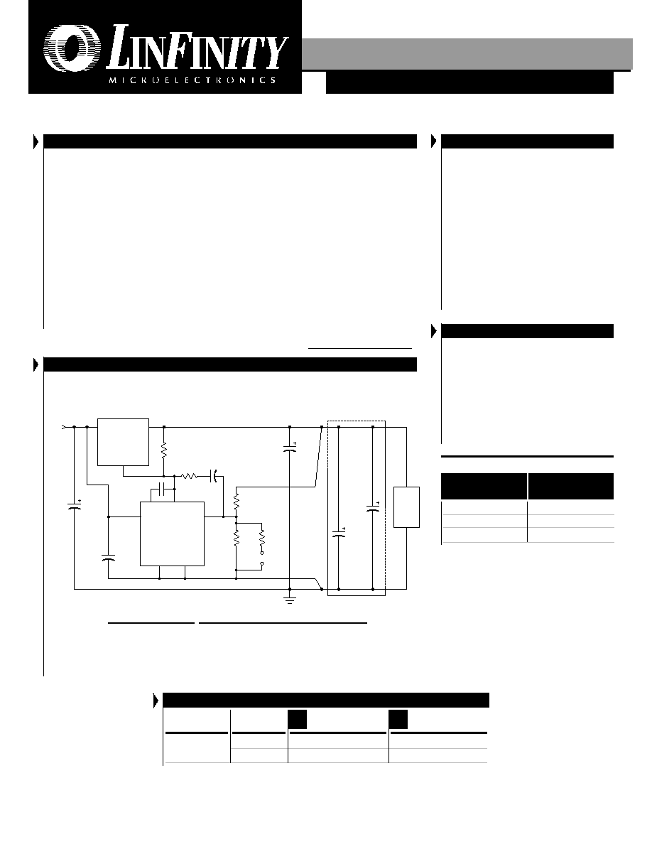
P R O D U C T H I G H L I G H T
T
HE
A
PPLICATION
OF
THE
LX8585A & LX1431
IN
A
75 & 166MH
Z
P54C P
ROCESSORS
U
SING
5V C
ACHE
µP
Load
100µF x 6
10V
AVX TYPE
TPS
1µF x 10
SMD
1k
0.1%
2.84k
0.1%
COL
V
+
V
+
V
+
SGND FGND
REF
LX1431
V
IN
V
OUT
ADJ
1k
1k
0.01µF
2x
330µF, 6.3V
Low ESR
Oscon Type
from Sanyo
2
3
1
6
5
8
1
3
0.1µF
50V
220µF
10V
Low ESR
from
Sanyo
5V
PLACE IN µP SOCKET CAVITY
LX8585A
2
250pF
21k
1%
JP1
V
O
4.6A
(See Table Below)
Thick traces represent high current traces which must be low resistance / low
inductance traces in order to achieve good transient response.
V
OUT
JP1
TYPICAL APPLICATION
3.50
Short
120/166MHz, VRE, 5V Cache
3.38
Open
75/90/100/133MHz, STND, 5V Cache
P A C K A G E O R D E R I N F O R M A T I O N
T
A
(∞C)
Plastic TO-220
3-pin
P
Plastic T0-263
3-pin
DD
0 to 125
1.4V
LX8585-xxCP
LX8585-xxCDD
1.2V
LX8585A-xxCP
LX8585A-xxCDD
Dropout
Voltage
Note: All surface-mount packages are available in Tape & Reel. Append the letter "T" to part number. (i.e. LX8585A-00CDDT)
"xx" refers to output voltage, please see table above.
LX8585/85A-00
Adjustable
LX8585/85A-15
1.5V
LX8585/85A-33
3.3V
Part #
Output
Voltage
A
VA I L A B L E
O
P T I O N S
P E R
P
A R T
#
Other voltage options may be available --
Please contact factory for details.
Copyright © 1997
Rev. 2.2 12/97
1
11861 W
ESTERN
A
VENUE
, G
ARDEN
G
ROVE
, CA. 92841, 714-898-8121, F
AX
: 714-893-2570
L
I N
F
I N I T Y
M
I C R O E L E C T R O N I C S
I
N C
.
IMPORTANT: For the most current data, consult LinFinity's web site: http://www.linfinity.com.
4 . 6 A L
O W
D
R O P O U T
P
O S I T I V E
R
E G U L A T O R S
LX8585-xx/8585A-xx
P R O D U C T D A T A B O O K 1 9 9 6 / 1 9 9 7
Copyright © 1997
Rev. 2.2 12/97
2
P
R O D U C T I O N
D
A T A
S
H E E T
ABSOLUTE MAXIMUM RATINGS
(Note 1)
Power Dissipation .................................................................................. Internally Limited
Input Voltage ................................................................................................................ 10V
Input to Output Voltage Differential ........................................................................... 10V
Operating Junction Temperature
Plastic (P, DD Package) ........................................................................................ 150∞C
Storage Temperature Range ...................................................................... -65∞C to 150∞C
Lead Temperature (Soldering, 10 seconds) ............................................................. 300∞C
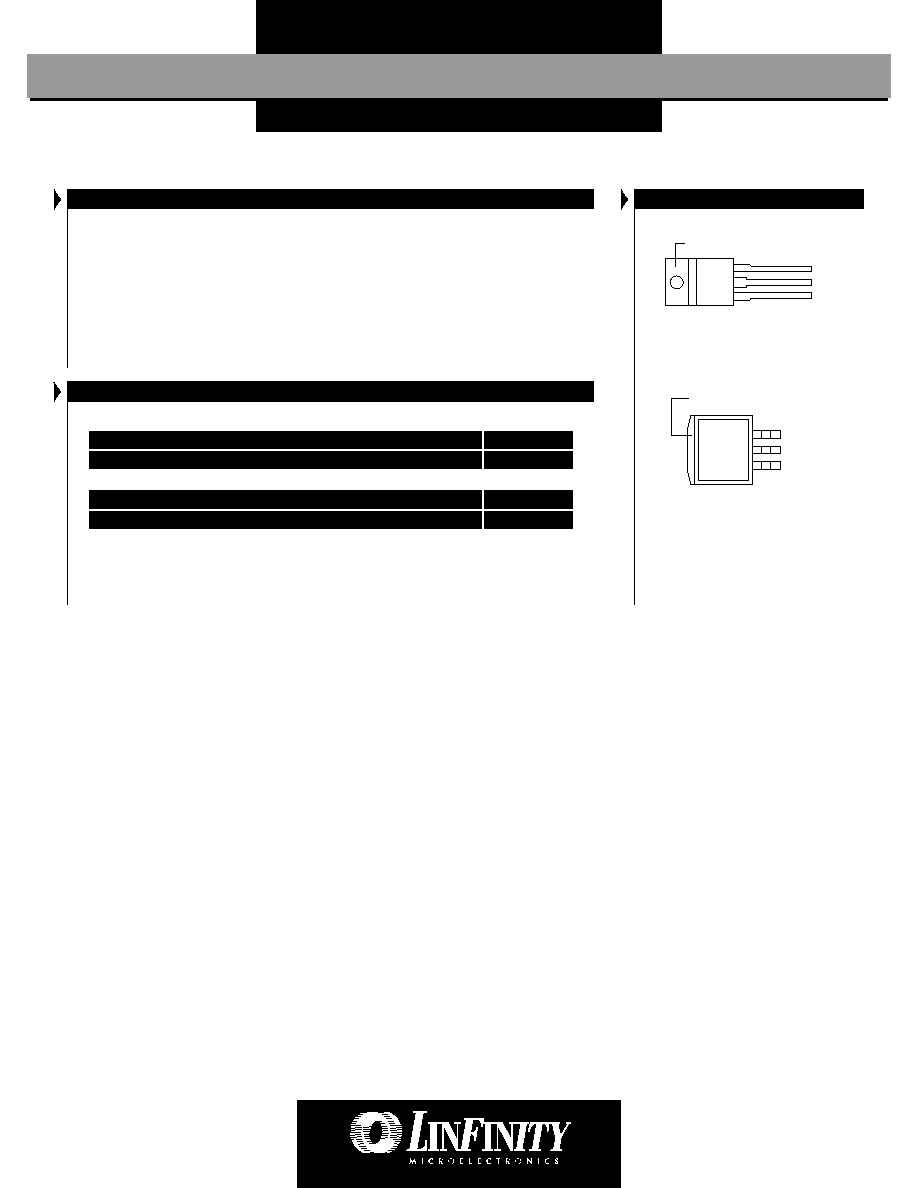
PACKAGE PIN OUTS
P PACKAGE
(Top View)
* Pin 1 is GND for fixed voltage versions.
3
2
1
V
IN
ADJ / GND*
V
OUT
DD PACKAGE
(Top View)
* Pin 1 is GND for fixed voltage versions.
Note 1. Exceeding these ratings could cause damage to the device. All voltages are with respect
to Ground. Currents are positive into, negative out of the specified terminal.
P PACKAGE:
THERMAL RESISTANCE-JUNCTION TO TAB,
JT
3.0∞C/W
THERMAL RESISTANCE-JUNCTION TO AMBIENT,
JA
60∞C/W
DD PACKAGE:
THERMAL RESISTANCE-JUNCTION TO TAB,
JT
3.0∞C/W
THERMAL RESISTANCE-JUNCTION TO AMBIENT,
JA
60∞C/W*
Junction Temperature Calculation: T
J
= T
A
+ (P
D
x
JA
). The
JA
numbers are guidelines for the
thermal performance of the device/pc-board system. All of the above assume no ambient airflow.
*
JA
can be improved with package soldered to 0.5IN
2
copper area over backside ground
plane or internal power plane.
JA
can vary from 20∫C/W to > 40∫C/W depending on
mounting technique.
THERMAL DATA
V
IN
V
OUT
ADJ / GND*
3
2
1
TAB IS V
OUT
TAB IS V
OUT
4 . 6 A L
O W
D
R O P O U T
P
O S I T I V E
R
E G U L A T O R S
LX8585-xx/8585A-xx
P R O D U C T D A T A B O O K 1 9 9 6 / 1 9 9 7
3
Copyright © 1997
Rev. 2.2 12/97
P
R O D U C T I O N
D
A T A
S
H E E T
Reference Voltage
LX8585/85A
V
REF
I
OUT
= 10mA, T
A
= 25∞C
10mA
I
OUT
4.6A, 1.5V
(V
IN
- V
OUT
), V
IN
7V, P
P
MAX
Line Regulation (Note 2)
V
REF
(V
IN
) I
OUT
= 10mA, 1.5V
(V
IN
- V
OUT
), V
IN
7V
Load Regulation (Note 2)
V
REF
(I
OUT
)
V
IN
- V
OUT
= 3V, 10mA
I
OUT
4.6A
Thermal Regulation
V
OUT
(Pwr)
T
A
= 25∞C, 20ms pulse
Ripple Rejection (Note 3)
V
OUT
= 3.3V, f =120Hz, C
OUT
= 100µf Tantalum, V
IN
= 5V
C
ADJ
= 10µF, T
A
= 25∞C, I
OUT
= 4.6A
Adjust Pin Current
I
ADJ
Adjust Pin Current Change
I
ADJ
10mA
I
OUT
4.6A, 1.5V
(V
IN
- V
OUT
), V
IN
7V
Dropout Voltage
LX8585
V
V
REF
= 1%, I
OUT
= 4.6A
V
REF
= 1%, I
OUT
= 3A
LX8585A
V
REF
= 1%, I
OUT
= 4.6A
Minimum Load Current
I
OUT(MIN)
V
IN
7V
Maximum Output Current (Note 4)
I
OUT(MAX)
1.4V
(V
IN
- V
OUT
), V
IN
7V
Temperature Stability (Note 3)
V
OUT
(t)
Long Term Stability (Note 3)
V
OUT
(t) T
A
= 125∞C, 1000 hrs
RMS Output Noise (% of V
OUT
) (Note 3) V
OUT (RMS)
T
A
= 125∞C, 10Hz
£ f £ 10kHz
E L E C T R I C A L C H A R A C T E R I S T I C S
(Unless otherwise specified, these specifications apply over the operating ambient temperatures for the LX8585-xxC/85A-xxC with 0∞C
T
A
125∞C;
V
IN
- V
OUT
= 3V; I
OUT
= 4.6A. Low duty cycle pulse testing techniques are used which maintains junction and case temperatures equal to the ambient temperature.)
Parameter
Symbol
Test Conditions
Units
LX8585/85A-00
Min.
Typ.
Max.
1.238
1.250
1.262
V
1.225
1.250
1.275
V
0.035
0.2
%
0.1
0.5
%
0.01
0.02
%/W
60
83
dB
55
100
µA
0.2
5
µA
1.2
1.4
V
1.1
1.3
V
1.1
1.2
V
2
10
mA
4.6
6
A
0.25
%
0.3
1
%
0.003
%
Note 2.
Regulation is measured at constant junction temperature, using pulse testing with a low duty cycle. Changes in output voltage due to heating
effects are covered under the specification for thermal regulation.
Note 3.
These parameters, although guaranteed, are not tested in production.
Note 4.
I
OUT (MAX)
is measured under the condition that V
OUT
is forced below its nominal value by 100mV.
Parameter
Symbol
Test Conditions
Units
LX8585/85A-15
Min.
Typ.
Max.
Output Voltage (Note 4)
V
OUT
V
IN
= 5V, I
OUT
= 0mA, T
A
= 25∞C
4.75V
V
IN
10V, 0mA
I
OUT
7A, T
A
= 25∞C, P
P
MAX
Line Regulation (Note 2)
V
OUT
4.75V
V
IN
7V
(V
IN
)
4.75V
V
IN
10V
Load Regulation (Note 2)
V
OUT
(I
OUT
)
V
IN
= 5V, 10mA
I
OUT
I
OUT (MAX)
Thermal Regulation (Note 3)
V
OUT
(Pwr)
T
A
= 25∞C, 20ms pulse
Ripple Rejection (Note 3)
C
OUT
= 100µF (Tantalum), I
OUT
= 4.6A, T
A
= 25∞C
Quiescent Current
I
Q
0mA
I
OUT
I
OUT (MAX)
, 4.75V
V
IN
10V
Dropout Voltage
LX8585-15
V
V
OUT
= 1%, I
OUT
I
OUT (MAX)
, V
IN
- V
OUT
7V
V
OUT
= 1%, I
OUT
3A, V
IN
- V
OUT
7V
LX8585A-15
V
OUT
= 1%, I
OUT
I
OUT (MAX)
, V
IN
- V
OUT
7V
Temperature Stability (Note 3)
V
OUT
(T)
Long Term Stability (Note 3)
V
OUT
(t) T
A
= 125∞C, 1000 hours
RMS Output Noise (% of V
OUT
) (Note 3) V
OUT (RMS)
T
A
= 25∞C, 10Hz
f
10kHz
1.485
1.50
1.515
V
1.470
1.50
1.530
V
1
3
mV
1
5
mV
2.5
7
mV
0.01
0.02
% / W
65
83
dB
4
10
mA
1.2
1.4
V
1.1
1.3
V
1.1
1.2
V
0.25
%
0.3
1
%
0.003
%
LX8585-00 / 8585A-00 (Adjustable)
LX8585-15 / 8585A-15 (1.5V Fixed)
4 . 6 A L
O W
D
R O P O U T
P
O S I T I V E
R
E G U L A T O R S
LX8585-xx/8585A-xx
P R O D U C T D A T A B O O K 1 9 9 6 / 1 9 9 7
Copyright © 1997
Rev. 2.2 12/97
4
P
R O D U C T I O N
D
A T A
S
H E E T
E L E C T R I C A L C H A R A C T E R I S T I C S
(Continued)
Parameter
Symbol
Test Conditions
Units
LX8585/85A-33
Min.
Typ.
Max.
Output Voltage (Note 4)
V
OUT
V
IN
= 5V, I
OUT
= 0mA, T
A
= 25∞C
4.75V
V
IN
10V, 0mA
I
OUT
7A, T
A
= 25∞C, P
P
MAX
Line Regulation (Note 2)
V
OUT
4.75V
V
IN
7V
(V
IN
)
4.75V
V
IN
10V
Load Regulation (Note 2)
V
OUT
(I
OUT
)
V
IN
= 5V, 10mA
I
OUT
I
OUT (MAX)
Thermal Regulation (Note 3)
V
OUT
(Pwr)
T
A
= 25∞C, 20ms pulse
Ripple Rejection (Note 3)
C
OUT
= 100µF (Tantalum), I
OUT
= 4.6A, T
A
= 25∞C
Quiescent Current
I
Q
0mA
I
OUT
I
OUT (MAX)
, 4.75V
V
IN
10V
Dropout Voltage
LX8585-33
V
V
OUT
= 1%, I
OUT
I
OUT (MAX)
, V
IN
- V
OUT
7V
V
OUT
= 1%, I
OUT
3A, V
IN
- V
OUT
7V
LX8585A-33
V
OUT
= 1%, I
OUT
I
OUT (MAX)
, V
IN
- V
OUT
7V
Temperature Stability (Note 3)
V
OUT
(T)
Long Term Stability (Note 3)
V
OUT
(t) T
A
= 125∞C, 1000 hours
RMS Output Noise (% of V
OUT
) (Note 3) V
OUT (RMS)
T
A
= 25∞C, 10Hz
f
10kHz
3.267
3.3
3.333
V
3.235
3.3
3.365
V
1
6
mV
2
10
mV
5
15
mV
0.01
0.02
% / W
65
83
dB
4
10
mA
1.2
1.4
V
1.1
1.3
V
1.1
1.2
V
0.25
%
0.3
1
%
0.003
%
LX8585-33 / 8585A-33 (3.3V Fixed)
4 . 6 A L
O W
D
R O P O U T
P
O S I T I V E
R
E G U L A T O R S
LX8585-xx/8585A-xx
P R O D U C T D A T A B O O K 1 9 9 6 / 1 9 9 7
5
Copyright © 1997
Rev. 2.2 12/97
P
R O D U C T I O N
D
A T A
S
H E E T
A P P L I C A T I O N N O T E S
The LX8585/85A Series ICs are easy to use Low-Dropout (LDO)
voltage regulators. They have all of the standard self-protection
features expected of a voltage regulator: short circuit protection, safe
operating area protection and automatic thermal shutdown if the
device temperature rises above approximately 165∞C.
Use of an output capacitor is REQUIRED with the LX8585/85A
series. Please see the table below for recommended minimum
capacitor values.
These regulators offer a more tightly controlled reference voltage
tolerance and superior reference stability when measured against
the older pin-compatible regulator types that they replace.
STABILITY
The output capacitor is part of the regulator's frequency compen-
sation system. Many types of capacitors are available, with different
capacitance value tolerances, capacitance temperature coefficients,
and equivalent series impedances. For all operating conditions,
connection of a 220µF aluminum electrolytic capacitor or a 47µF
solid tantalum capacitor between the output terminal and ground
will guarantee stable operation.
If a bypass capacitor is connected between the output voltage
adjust (ADJ) pin and ground, ripple rejection will be improved
(please see the section entitled "RIPPLE REJECTION"). When ADJ
pin bypassing is used, the required output capacitor value increases.
Output capacitor values of 220µF (aluminum) or 47µF (tantalum)
provide for all cases of bypassing the ADJ pin. If an ADJ pin bypass
capacitor is not used, smaller output capacitor values are adequate.
The table below shows recommended minimum capacitance values
for stable operation.
INPUT
OUTPUT
ADJ
10µF
15µF Tantalum, 100µF Aluminum
None
10µF
47µF Tantalum, 220µF Aluminum
15µF
To ensure good transient response from the power supply system
under rapidly changing current load conditions, designers generally
use several output capacitors connected in parallel. Such an
arrangement serves to minimize the effects of the parasitic resistance
(ESR) and inductance (ESL) that are present in all capacitors. Cost-
effective solutions that sufficiently limit ESR and ESL effects gener-
ally result in total capacitance values in the range of hundreds to
thousands of microfarads, which is more than adequate to meet
regulator output capacitor specifications. Output capacitance
values may be increased without limit.
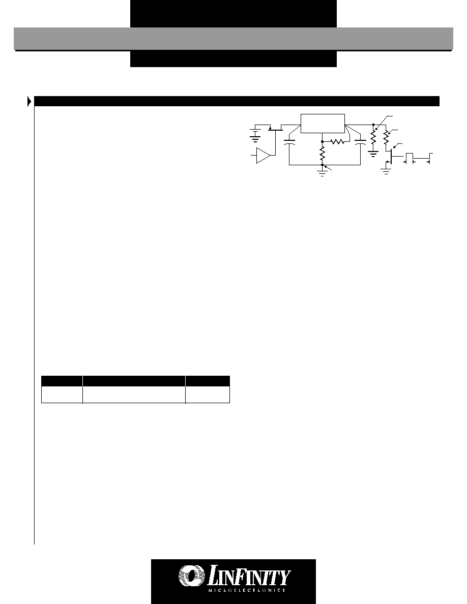
The circuit shown in Figure 1 can be used to observe the transient
response characteristics of the regulator in a power system under
changing loads. The effects of different capacitor types and values
on transient response parameters, such as overshoot and under-
shoot, can be compared quickly in order to develop an optimum
solution.
RECOMMENDED CAPACITOR VALUES
FIGURE 1 -- DYNAMIC INPUT and OUTPUT TEST
LX8585/85A
Power Supply
OUT
IN
ADJ
Star Ground
1 sec
10ms
R
DSON
<< R
L
Full Load
(Smaller resistor)
Minumum Load
(Larger resistor)
OVERLOAD RECOVERY
Like almost all IC power regulators, the LX8585/85A regulators are
equipped with Safe Operating Area (SOA) protection. The SOA
circuit limits the regulator's maximum output current to progres-
sively lower values as the input-to-output voltage difference
increases. By limiting the maximum output current, the SOA circuit
keeps the amount of power that is dissipated in the regulator itself
within safe limits for all values of input-to-output voltage within the
operating range of the regulator. The LX8585/85A SOA protection
system is designed to be able to supply some output current for all
values of input-to-output voltage, up to the device breakdown
voltage.
Under some conditions, a correctly operating SOA circuit may
prevent a power supply system from returning to regulated
operation after removal of an intermittent short circuit at the output
of the regulator. This is a normal mode of operation which can be
seen in most similar products, including older devices such as 7800
series regulators. It is most likely to occur when the power system
input voltage is relatively high and the load impedance is relatively
low.
When the power system is started "cold", both the input and
output voltages are very close to zero. The output voltage closely
follows the rising input voltage, and the input-to-output voltage
difference is small. The SOA circuit therefore permits the regulator
to supply large amounts of current as needed to develop the
designed voltage level at the regulator output.
Now consider the case where the regulator is supplying regulated
voltage to a resistive load under steady state conditions. A moderate
input-to-output voltage appears across the regulator but the voltage
difference is small enough that the SOA circuitry allows sufficient
current to flow through the regulator to develop the designed output
voltage across the load resistance. If the output resistor is short-
circuited to ground, the input-to-output voltage difference across the
regulator suddenly becomes larger by the amount of voltage that had
appeared across the load resistor. The SOA circuit reads the increased
input-to-output voltage, and cuts back the amount of current that it will
permit the regulator to supply to its output terminal. When the short
circuit across the output resistor is removed, all the regulator output
current will again flow through the output resistor. The maximum
current that the regulator can supply to the resistor will be limited by
the SOA circuit, based on the large input-to-output voltage across the
regulator at the time the short circuit is removed from the output.