Microsemi
Linfinity Microelectronics Division
11861 Western Avenue, Garden Grove, CA. 92841, 714-898-8121, Fax: 714-893-2570
Page 1
Copyright
©
2000
Rev. 0.2a, 2000-11-20
WWW.
Microsemi
.
COM
LX8815
Dual Channel 1A Low Dropout Regulator
P
RELIMINARY
A M I C R O S E M I C O M P A N Y
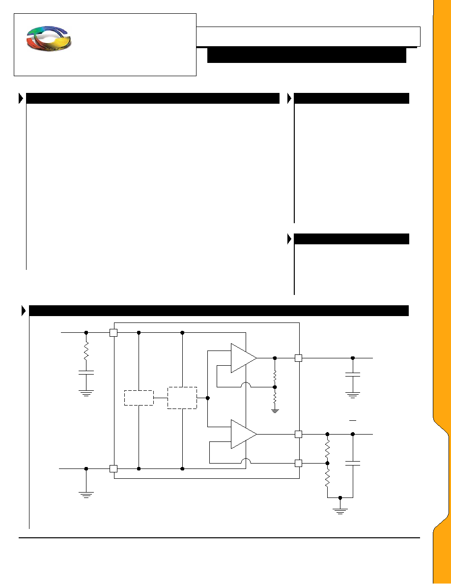
The LX8815 is a dual channel
positive-voltage linear regulator. This
dual regulator has either one fixed
output coupled with an adjustable
output or two fixed outputs. Each
channel features low-dropout and high
accuracy.
The LX8815 provides designers
with a flexible power management
solution, minimal printed circuit board
area, and shorter design cycles.
Each channel can supply up to one
amp independently with a regulator
design optimized for system efficiency
by consuming minimal ground current
and directing quiescent current to the
load.
The LX8815 features on-chip
trimming of the internal
voltage reference enabling precise output
voltages, typically
±
1% of it's specified
value, while the BiPolar output transistor
has a low dropout voltage even at full
output current (V
DO
< 1.1V typ. @ 1A).
Thermal and Short Circuit Current
Protection are integrated on-chip and
operate independently for each regulator
output.
The LX8815 regulator is stable with a
low-value output capacitor, typically
3.3
µ
F tantalum or 4.7
µ
F ceramic on the
outputs, allowing designers flexibility in
external component selection.
Linfinity's S-PAK power package
offers maximum power dissipation and
ease of assembly using surface mount
technology.
IMPORTANT:
For the most current data, consult
MICROSEMI
's website: http://www.microsemi.com
�
�
Two Independent Regulated
Outputs
Accurate Output Voltages
Max. Dropout of 1.1V at Rated
Current
Independent Thermal and
Current Limit Protection
Low Profile 5 Lead SMT Power
Package
Low Tolerance Line (0.2%) and
Load (0.4%) Regulation
Wide DC Supply Voltage of 4.0V
to 12.0V
Loop Stability Independent of
Output Capacitor Type
5V to 3.3V Linear Regulator
Low Voltage Logic Supplies
Active SCSI Terminators
Battery Charging Circuits
Instrumentation
PC Peripherals
�
�
B I A S
1 . 2 5 V
V
R E F
1
3
V
I N
G N D
5
4
2
+
+
-
-
V
O U T 1
V
O U T 2
R
3
0.1
C
1
1 0
µ
F
C
2
4.7
µ
F
R
1
R
2
C
3
4.7
µ
F
2
2
1
2
1
25
.
1
R
I
R
R
V
ADJ
OUT
◊
+
+
◊
=
Note: Application circuit above using ceramic capacitors, C
1
requires R
3
(0.075 to 0.3
). For Tantalum capacitors: R
3
is not used
a n d C
1
, C
2
, and C
3
> 2
µ
F. R1 and R2 used with LX88xx-xx only.
Adjustable or Fixed
L
L
X
X
8
8
8
8
1
1
5
5
Microsemi
Linfinity Microelectronics Division
11861 Western Avenue, Garden Grove, CA. 92841, 714-898-8121, Fax: 714-893-2570
Page 2
Copyright
©
2000
Rev. 0.2a, 2000-11-20
WWW.
Microsemi
.
COM
LX8815
Dual Channel 1A Low Dropout Regulator
P
RELIMINARY
A M I C R O S E M I C O M P A N Y
�
T
J
(
∞
C)
O
UTPUT
V
1
O
UTPUT
V
2
DF
Plastic S-PAK
5-PIN
3.3V 2.5V
LX8815-3325CDF
3.3V 1.8V
LX8815-3318CDF
3.3V Adj
LX8815-3300CDF
2.85V Adj
LX8815-2800CDF
0 to 125
2.5V Adj
LX8815-2500CDF
Note: Available in Tape & Reel.
Append the letter "T" to the part number. (i.e. LX8815-3325CDFT)
DF
P
ACKAGE
THERMAL RESISTANCE
-
JUNCTION TO
T
AB
,
JT
THERMAL RESISTANCE
-
JUNCTION TO
A
MBIENT
,
JA
4.5
∞
C/W
24.5
∞
C/W
Junction Temperature Calculation: T
J
= T
A
+ (P
D
x
JA
).
The
JA
numbers are guidelines for the thermal performance of the device/pc-board
system. All of the above assume no ambient airflow.
JA
can vary from 20
∞
C/W to >
40
∞
C/W depending on mounting technique. (See Application Notes Section: Thermal
considerations)
�
�
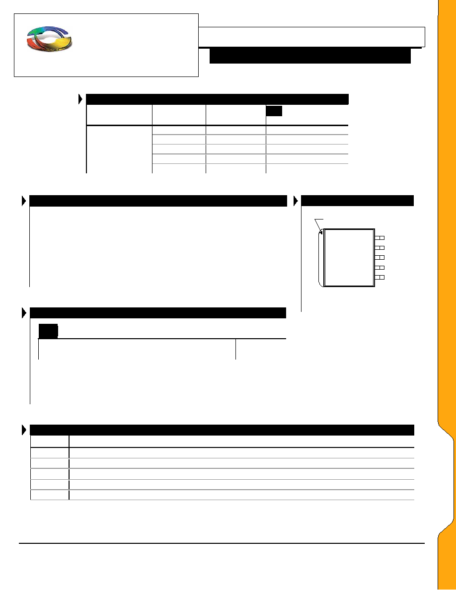
D F P
A C K A G E
( T op V ie w)
1
V
IN
A D J
G N D
V
OUT2
V
OUT1
2
3
4
5
TAB is GND
�
V
IN
Unregulated input voltage supply.
ADJ
Adjust control pin for regulator 2
GND
Common terminal for ground reference
V
OUT1
Fixed voltage regulator output (Regulator #1)
V
OUT2
Fixed or adjustable regulator output (Regulator #2)
Input Voltage (V
BAT
) ..................................................................................................13.5V
Load Current (Internally Limited)................................................................................... 1A
Power Dissipation ................................................................................... Internally Limited
Short-Circuit Protection ....................................................................................... Indefinite
Operating Junction Temperature ................................................................................150
∞
C
Lead Temperature (Soldering 180 seconds) ...............................................................235
∞
C
Note:
Exceeding these ratings could cause damage to the device. All voltages are with respect to
Ground. Currents are positive into, negative out of specified terminal.
P
P
A
A
C
C
K
K
A
A
G
G
E
E
D
D
A
A
T
T
A
A
Microsemi
Linfinity Microelectronics Division
11861 Western Avenue, Garden Grove, CA. 92841, 714-898-8121, Fax: 714-893-2570
Page 3
Copyright
©
2000
Rev. 0.2a, 2000-11-20
WWW.
Microsemi
.
COM
LX8815
Dual Channel 1A Low Dropout Regulator
P
RELIMINARY
A M I C R O S E M I C O M P A N Y
Unless otherwise specified, the following specifications apply over the operating ambient temperature 0
∞
C
T
A
125
∞
C except where
otherwise noted and the following test conditions: V
IN
= 5V, I
OUT
= 10mA, C
1
= 4.7
µ
F (Tantalum), C
2
= 4.7
µ
F (Tantalum), and T
J
= T
A
25
∞
C using low duty cycling methods.
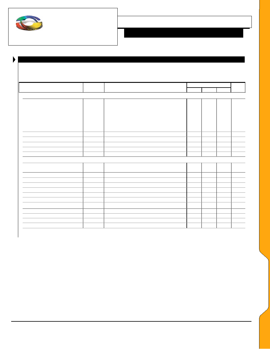
LX8815-xx00
Parameter Symbol
Test
Conditions
Min Typ Max
Units
FIXED OUTPUT
Output Voltage
∑
LX8815-3300
∑
LX8815-2800
∑
LX8815-2500
V
1
V
IN
= 5V, I
OUT
= 5mA, T
J
= 25
∞
C
5mA < I
1
< 1A, 4.50V < V
IN
< 10V
V
IN
= 5V, I
OUT
= 5mA, T
J
= 25
∞
C
5mA < I
1
< 1A, 4.50V < V
IN
< 10V
V
IN
= 5V, I
OUT
= 5mA, T
J
= 25
∞
C
5mA < I
1
< 1A, 4.50V < V
IN
< 10V
3.250
3.234
2.807
2.793
2.462
2.450
3.300
3.300
2.850
2.850
2.500
2.500
3.350
3.366
2.893
2.907
2.537
2.550
V
Line Regulation
V
1
(V
IN
)
4.75V < V
IN
< 10V, I
OUT
= 5mA
0.01
0.2
%V
1
Load Regulation
V
1
(I
1
)
5mA < I
1
< 1A, V
IN
= 4.75V
0.01
0.4
%V
1
Dropout Voltage
V I
LOAD
= 1A,
V
1
= -2%
1.1
1.25
V
Current Limit
I
OUT (MAX)
(V
IN
≠ V
1
) = 5V
1.0
1.4
A
Minimum Load Current
I
L
Note 1
0
2
mA
ADJUSTABLE OUTPUT
Reference Voltage
V
REF
V
IN
= 5V, I
OUT
= 10mA, T
J
= 25
∞
C
5mA < I
1
< 1A, 4.50V < V
IN
< 10V
1.238
1.231
1.250
1.250
1.262
1.269
V
Line Regulation
V
REF
(V
IN
) 4.75V < V
IN
< 10V, I
OUT
= 5mA
0.01
0.2
%V
1
Load Regulation
V
REF
(I
2
) 5mA < I
1
< 1A, V
IN
= 4.75V
0.01
0.4
%V
1
Dropout Voltage
V V
IN
> 4.5V, I
LOAD
= 1A,
V
1
= -1%
1.1
1.3
V
Current Limit
I
OUT (MAX)
(V
IN
≠ V
1
) = 5V
1.0
1.4
A
Minimum Load Current
I
L
Note 1
1
3
mA
Adjust Pin Bias Current
I
ADJ
1
5
µ
A
ENTIRE REGULATOR
Quiescent Current
I
Q
V
IN
< 10V, I
1
= 5mA, I
2
= 5mA
1.8
5
mA
Ripple Rejection
PSRR
f=120Hz, V
IN
= 5V
60
75
dB
RMS Output Noise (% of V
OUT
) V
OUT (RMS)
10Hz < f < 10kHz
0.003
%V
1
Thermal Shutdown
T
JSD
140
∞
C
Note 1: Minimum load current is defined as the amount of output current required to maintain regulation.
E
E
L
L
E
E
C
C
T
T
R
R
I
I
C
C
A
A
L
L
S
S
Microsemi
Linfinity Microelectronics Division
11861 Western Avenue, Garden Grove, CA. 92841, 714-898-8121, Fax: 714-893-2570
Page 4
Copyright
©
2000
Rev. 0.2a, 2000-11-20
WWW.
Microsemi
.
COM
LX8815
Dual Channel 1A Low Dropout Regulator
P
RELIMINARY
A M I C R O S E M I C O M P A N Y
Unless otherwise specified, the following specifications apply over the operating ambient temperature 0
∞
C
T
A
125
∞
C except where
otherwise noted and the following test conditions: V
IN
= 5V, I
OUT
= 10mA, C
1
= 4.7
µ
F (Tantalum), C
2
= 4.7
µ
F (Tantalum), and T
J
= T
A
25
∞
C using low duty cycling methods.
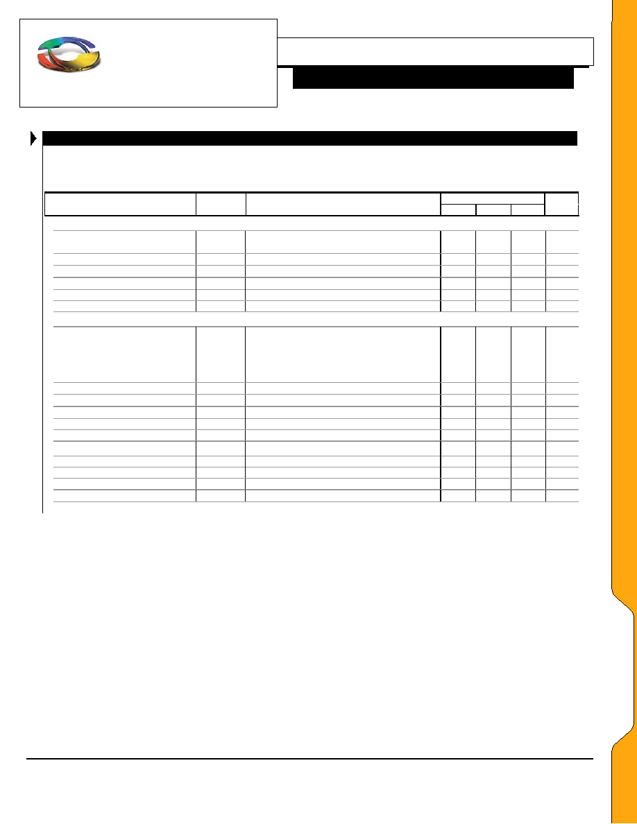
LX8815-33xx
Parameter Symbol
Test
Conditions
Min Typ Max
Units
FIXED OUTPUT 1
Output Voltage
V
1
V
IN
= 5V, I
OUT
= 5mA, T
J
= 25
∞
C
5mA < I
1
< 1A, 4.50V < V
IN
< 10V
3.250
3.234
3.300
3.300
3.350
3.366
V
Line Regulation
V
1
(V
IN
)
4.75V < V
IN
< 10V, I
OUT
= 5mA
0.3
5.0
mV
Load Regulation
V
1
(I
1
)
5mA < I
1
< 1A, V
IN
= 4.75V
0.8
10
mV
Dropout Voltage
V I
LOAD
= 1A,
V
1
= -2%
1.1
1.25
V
Current Limit
I
OUT (MAX)
(V
IN
≠ V
1
)
1.0
1.4 A
Minimum Load Current
I
L
Note 1
0
2
mA
FIXED OUTPUT 2
Output Voltage
∑
LX8815-3325
∑
LX8815-3318
V
1
V
IN
= 5V, I
OUT
= 5mA, T
J
= 25
∞
C
5mA < I
1
< 1A, 4.50V < V
IN
< 10V
V
IN
= 5V, I
OUT
= 5mA, T
J
= 25
∞
C
5mA < I
1
< 1A, 4.50V < V
IN
< 10V
2.462
2.450
1.773
1.764
2.50
2.50
1.80
1.80
2.537
2.550
1.827
1.36
V
Line Regulation
V
1
(V
IN
)
4.75V < V
IN
< 10V, I
OUT
= 5mA
0.02
0.15
%mV
Load Regulation
V
1
(I
1
)
5mA < I
1
< 1A, V
IN
= 4.75V
0.04
0.3
%mV
Dropout Voltage
V V
IN
> 4.5V, I
LOAD
= 1A,
V
1
= -1%
1.1
1.3
V
Current Limit
I
OUT (MAX)
(V
IN
≠ V
1
)
1.0
1.4 A
Minimum Load Current
I
L
Note 1
1
2
mA
ENTIRE REGULATOR
Quiescent Current
I
Q
V
IN
< 10V, I
1
= 5mA, I
2
= 5mA
1.8
7
mA
Ripple Rejection
PSRR
f=120Hz, V
IN
= 5V
60
75
dB
RMS Output Noise (% of V
OUT
) V
OUT (RMS)
10Hz < f < 10kHz
0.003
%V
1
Thermal Shutdown
T
JSD
140
∞
C
Note 1: Minimum load current is defined as the amount of output current required to maintain regulation.
E
E
L
L
E
E
C
C
T
T
R
R
I
I
C
C
A
A
L
L
S
S
Microsemi
Linfinity Microelectronics Division
11861 Western Avenue, Garden Grove, CA. 92841, 714-898-8121, Fax: 714-893-2570
Page 5
Copyright
©
2000
Rev. 0.2a, 2000-11-20
WWW.
Microsemi
.
COM
LX8815
Dual Channel 1A Low Dropout Regulator
P
RELIMINARY
A M I C R O S E M I C O M P A N Y
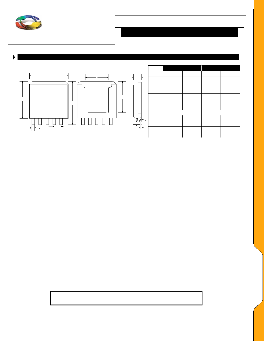
A
B
K
F
G
I
D
J
H
C
E
Note:
1. Dimensions do not include mold flash or protrusions;
these shall not exceed 0.155mm(.006") on any side.
Lead dimension shall not include solder coverage.
M
ILLIMETERS
I
NCHES
Dim
MIN MAX MIN MAX
A 9.27 9.52 .365 .375
B 8.89 9.14 .350 .360
C 1.77 2.03 .070 .080
D 7.49 7.74 .295 .305
E 0.12 0.38 .005 .015
F 0.58 0.84 .023 .033
G
1.70 BSC
0.067 BSC
H 0.79 1.04 .031 .041
I 4.31 6.86 .170 .270
J 0.03 0.13 .001 .005
K 10.41
10.67 .410 .420
Preliminary Data ≠ Information contained in this document is pre-production data and is proprietary to LinFinity. It
may not be modified in any way without the express written consent of LinFinity. Product referred to herein is offered
in sample form only and LinFinity reserves the right to change or discontinue this proposed product at any time.
M
M
E
E
C
C
H
H
A
A
N
N
I
I
C
C
A
A
L
L
S
S