Microsemi
Integrated Products
11861 Western Avenue, Garden Grove, CA. 92841, 714-898-8121, Fax: 714-893-2570
Page 1
Copyright
2000
Rev. 1.2a, 2002-11-01
WWW
.
Microse
m
i
.
CO
M
LX8816
Dual Channel 1A Low Dropout Regulator
P
RODUCTION
D
ATA
S
HEET
I N T E G R A T E D P R O D U C T S
D E S C R I P T I O N
The LX8816 is a dual channel
positive-voltage linear regulator. This
dual regulator has one fixed output
coupled with an adjustable output.
Each channel features low-dropout
and high accuracy.
The LX8816 provides designers
with a flexible power management
solution, minimal printed circuit board
area and shorter design cycles.
Each channel can supply up to one
amp independently with a regulator
design optimized for system efficiency
by consuming minimal ground current
and directing quiescent current to the
load.
The LX8816 features on-chip
trimming of the internal voltage
enabling precise output voltages,
typically
±1% of it's specified value,
while the BiPolar output transistor has a
low dropout voltage even at full output
current (V
DO
< 1.2V typ. @ 1A).
Thermal and Short Circuit Current
Protection are integrated on-chip and
operate independently for each regulator
output.
The LX8816 regulator is stable with a
low-value output capacitor, typically
2.2
µF on the outputs, allowing designers
flexibility in external component
selection.
Microsemi's S-PAK package enables
maximum power dissipation and ease of
assembly using surface mount
technology.
IMPORTANT:
For the most current data, consult
MICROSEMI
's website: http://www.microsemi.com
K E Y F E A T U R E S
Two Independent Regulated
Outputs
Accurate Output Voltages
Typical Dropout of 1.2V at 1A
and 1.1V at 500mA
Independent Thermal and
Current Limit Protection
Low Profile 5 Lead SMT Power
Package
Low Tolerance Load Regulation
Wide DC Supply Voltage of 4.3V
to 10V
Loop Stability Independent of
Output Capacitor Type
APPLICATIONS/BENEFITS
5V to 3.3V / ADJ Regulators
Hard Disk Drives, CD-ROMs
ADSL and Cable Modems
Battery Charging Circuits
Instrumentation
PC Peripherals
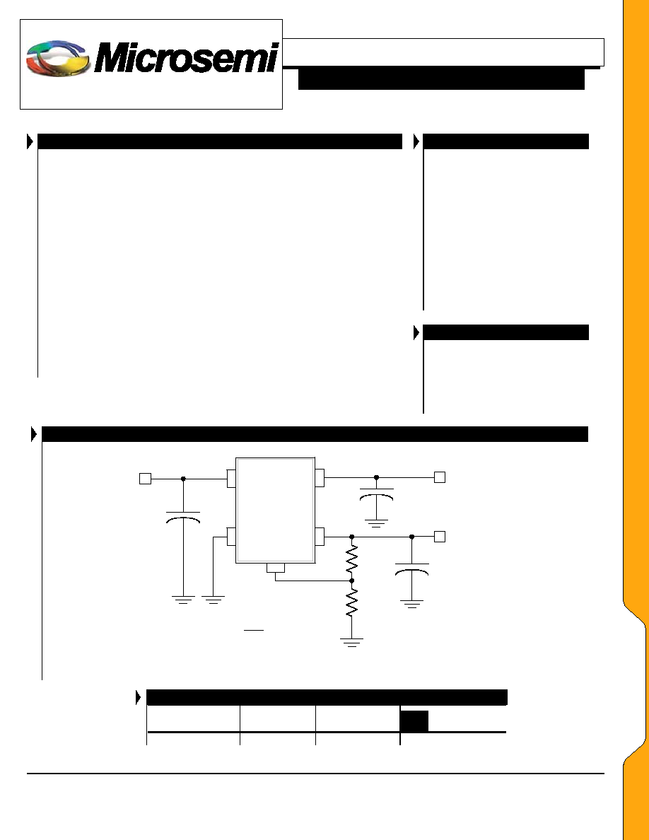
A P P L I C A T I O N C I R C U I T S
V
1
V
2
GND
ADJ
V
IN
LX8816-04
22µF
10µF
10 µF
V
IN
= 5V
3.3V @ 1.0A
2.5V* @ 1.0A
R1
499
R2
499
1
2
1
1
*
1
R
I
R
R
V
V
ADJ
REF
+
+
=
PACKAGE ORDER INFO
T
J
(
∞C)
O
UTPUT
V
1
(PIN
4)
O
UTPUT
V
2
(PIN
5)
DF
Plastic S-PAK
5-PIN
0 to 125
Adj.
3.3V
LX8816-04CDF
Note: Available in Tape & Reel.
Append the letter "T" to the part number. (i.e. LX8816-04CDFT)
L
L
X
X
8
8
8
8
1
1
6
6
Microsemi
Integrated Products
11861 Western Avenue, Garden Grove, CA. 92841, 714-898-8121, Fax: 714-893-2570
Page 2
Copyright
2000
Rev. 1.2a, 2002-11-01
WWW
.
Microse
m
i
.
CO
M
LX8816
Dual Channel 1A Low Dropout Regulator
P
RODUCTION
D
ATA
S
HEET
I N T E G R A T E D P R O D U C T S
A B S O L U T E M A X I M U M R A T I N G S
Input Voltage (V
BAT
).................................................................................................. 13.5V
Load Current (Internally Limited)................................................................................... 1A
Power Dissipation ................................................................................... Internally Limited
Short-Circuit Protection ....................................................................................... Indefinite
Operating Junction Temperature ................................................................................150
∞C
Lead Temperature (Soldering 180 seconds)...............................................................235
∞C
Note:
Exceeding these ratings could cause damage to the device. All voltages are with respect to
Ground. Currents are positive into, negative out of specified terminal.
T H E R M A L D A T A
DF
Plastic S-Pak 5-Pin
T
HERMAL
R
ESISTANCE
-J
UNCTION TO
T
AB
,
JT
4.5∞C/W
T
HERMAL
R
ESISTANCE
-J
UNCTION TO
A
MBIENT
,
J
A
24.5∞C/W
Junction Temperature Calculation: T
J
= T
A
+ (P
D
x
JA
).
The
JA
numbers are guidelines for the thermal performance of the device/pc-board
system. All of the above assume no ambient airflow.
JA
can vary from 25
∞C/W to >
40
∞C/W depending on mounting technique. (See Application Notes Section: Thermal
considerations)
PACKAGE PIN OUT
1
2
3
4
5
V
2
V
1
GND
ADJ
V
IN
Tab is GND
DF P
ACKAGE
(Top View)
F U N C T I O N A L P I N D E S C R I P T I O N
P
IN
N
AME
D
ESCRIPTION
V
IN
Positive unregulated supply input for the regulator. Bypass to GND with at least 2.2µF capacitance having low
ESR for good transient response.
ADJ
Adjustable Input
.
The output voltage can be set by two external resistors with the following relationship: V
1
= V
REF
* (1 + R1 / R2) + I
ADJ
* R1 where R1 is the resistor connected between V
1
and ADJ, and R2 is the resistor
connected between ADJ and GND.
GND
Common terminal for ground reference.
The input and output bypass capacitors should be connected to this
pin. In addition the tab on the S-Pak package and pin 3 are also used for heat sinking the device.
V
1
Adjustable regulator output (Regulator #1) It is recommended to bypass to GND with at least 2.2uF. Size your
output capacitor to meet the transient loading requirement. If you have a very dynamic load, a lower ESR
capacitor will improve the response to these load steps.
V
2
Fixed regulator output (Regulator #2). It is recommended to bypass to GND with at least 2.2µF. Size your output
capacitor to meet the transient loading requirement. For dynamic loads, a lower ESR capacitor will improve the
response to these load steps.
P
P
A
A
C
C
K
K
A
A
G
G
E
E
D
D
A
A
T
T
A
A
Microsemi
Integrated Products
11861 Western Avenue, Garden Grove, CA. 92841, 714-898-8121, Fax: 714-893-2570
Page 3
Copyright
2000
Rev. 1.2a, 2002-11-01
WWW
.
Microse
m
i
.
CO
M
LX8816
Dual Channel 1A Low Dropout Regulator
P
RODUCTION
D
ATA
S
HEET
I N T E G R A T E D P R O D U C T S
R E C O M M E N D E D O P E R A T I N G C O N D I T I O N S
LX8816-04
Parameter Symbol
Min Typ Max
Units
Input Voltage
V
IN
4.5 10 V
Output Voltage (adjustable)
V
OUT
5.5
V
Load Current each output (with adequate heat sinking)
0
1000
mA
Input Capacitor (V
IN
to GND)
2.2
20
µF
Output Capacitor (V
OUT
to GND)
1.0
10*
µF
*
Size your output capacitor to meet the transient loading requirement. If you have a very dynamic load, a lower ESR and larger value capacitor will
improve the response to these load steps.
E L E C T R I C A L C H A R A C T E R I S T I C S
Unless otherwise specified, the following specifications apply over the operating ambient temperature 0
∞C
T
A
125
∞C except where
otherwise noted and the following test conditions: V
IN
= 5V, I
OUT
= 10mA, C
1
= 10
µF (Tantalum), C
2
= C
3
= 4.7
µF (Tant.), & T
J
= T
A
using
low duty cycling methods.
LX8816-04
Parameter Symbol
Test
Conditions
Min Typ Max
Units
Adjustable Output (Output 1)
Reference Voltage
V
REF
5mA < I
1
< 1A, 4.75V < V
IN
< 10V
1.225
1.25
1.273
V
Line Regulation
V
1
(V
IN
)
4.75V < V
IN
< 5.5V, I
OUT
= 5mA
1.5
2.5
mV
Line Regulation
V
1
(V
IN
)
4.50V < V
IN
< 10V, I
OUT
= 5mA
0.17
0.22
%V
Load Regulation
V
REF
(I
1
)
5mA < I
1
< 1A, V
IN
= 4.75V
0.04
0.15
%V
Dropout Voltage
V I
LOAD
= 1A,
V
1
= -2%
1.2
1.3 V
Current Limit
I
OUT (MAX)
1.0
1.4
A
Minimum Load Current
I
L
Note 1, The external resistor divider current can be
included in this requirement.
2 3
mA
Adjust Pin Bias Current
I
ADJ
Bias current flows into part.
0.12
1
µ
A
Fixed Output (Output 2)
Output Voltage
V
2
5mA < I
2
< 1A, 4.75V < V
IN
< 10V
3.234
3.30
3.3825
V
Line Regulation
V
2
(V
IN
)
4.75V < V
IN
< 5.5V, I
OUT
= 5mA
6
8
mV
Line Regulation
V
2
(V
IN
)
4.50V < V
IN
< 10V, I
OUT
= 5mA
0.17
0.22
%V
Load Regulation
V
2
(I
2
)
5mA < I
2
< 1A, V
IN
= 4.75V
2.6
6
mV
Dropout Voltage
V I
LOAD
= 1A,
V
2
= -2%
1.2
1.3 V
Current Limit
I
OUT (MAX)
1.0
1.4
A
Minimum Load Current
I
L
Note 1
0
mA
Entire Regulator
Quiescent Current
I
Q
V
IN
< 10V, I
1
= 5mA, I
2
= 5mA
2.6
3.8
mA
Quiescent Current
IQ
V
IN
< 10V, I
1
= 1A, I
2
= 1A
3.5
6
mA
Ripple Rejection
PSRR
f=120Hz, V
IN
= 5V
60
75
dB
RMS Output Noise (% of V
OUT
) V
OUT (RMS)
10Hz < f < 10kHz
0.003
%V
Thermal Shutdown
T
JSD
135
140
∞
C
Note 1: Minimum load current is defined as the amount of output current required to maintain regulation.
E
E
L
L
E
E
C
C
T
T
R
R
I
I
C
C
A
A
L
L
S
S
Microsemi
Integrated Products
11861 Western Avenue, Garden Grove, CA. 92841, 714-898-8121, Fax: 714-893-2570
Page 4
Copyright
2000
Rev. 1.2a, 2002-11-01
WWW
.
Microse
m
i
.
CO
M
LX8816
Dual Channel 1A Low Dropout Regulator
P
RODUCTION
D
ATA
S
HEET
I N T E G R A T E D P R O D U C T S
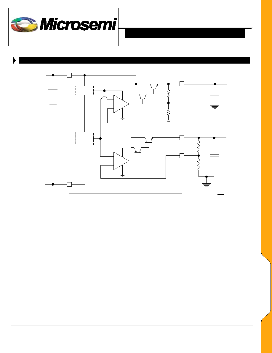
B L O C K D I A G R A M
BIAS
1.25V
V
REF
1
V
IN
4
2
V
OUT1
C
1
10
µ
F
R
1
R
2
C
3
10
µ
F
1
2
1
1
25
.
1
1
R
ADJ
I
R
R
OUT
V
◊
+
+
◊
=
Note: Application circuit above using ceramic capacitors. R1 and R2 used with adjustable version only.
(Adjustable)
+
-
5
V
OUT2
C
2
10
µ
F
GND
3
+
-
V
IN
(Fixed)
Figure 1 ≠ Simplified Block Diagram
B
B
L
L
O
O
C
C
K
K
D
D
I
I
A
A
G
G
R
R
A
A
M
M
Microsemi
Integrated Products
11861 Western Avenue, Garden Grove, CA. 92841, 714-898-8121, Fax: 714-893-2570
Page 5
Copyright
2000
Rev. 1.2a, 2002-11-01
WWW
.
Microse
m
i
.
CO
M
LX8816
Dual Channel 1A Low Dropout Regulator
P
RODUCTION
D
ATA
S
HEET
I N T E G R A T E D P R O D U C T S
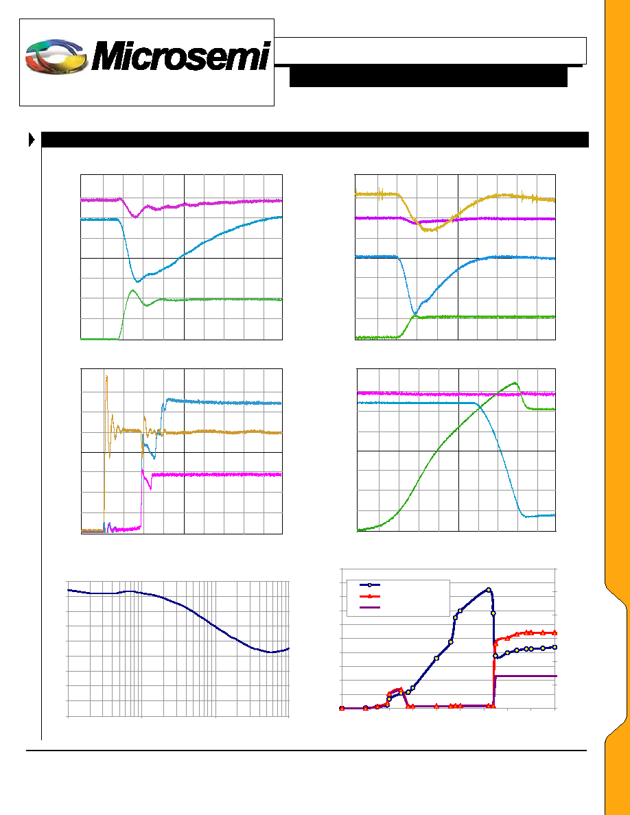
C H A R A C T E R I S T I C C U R V E S
LOAD TRANSIENT RESPONSE
V
IN
= 20µF Ceramic, ESR= 45m; V1,V2 = 10µF Ceramic, ESR= 75m
50mV
/ DIV
2µs / DIV
50mV
/ DIV
1A
V2 = 3.3V 1A Step Load
V1 = 1.5V 180
Load
1mA
LOAD TRANSIENT RESPONSE
V
IN
= 22µF Tantalum, ESR=232m; V1,V2 = 10µF Tantalum, ESR=198m
50mV
/ DIV
2µs / DIV
50mV
/ DIV
1A
V
IN
= 5V
0mA
V1 = 1.5V
V2 = 3.3V 1A Step Load
50mV
/ DIV
TURN ON CHARACTERISTICS
500mV
/ DIV
100µs / DIV
1V /
DIV
V2 = 3.3V
V
IN
= 5V
V1 = 1.5V
500m
V / DIV
CURRENT LIMIT RESPONSE
20mV(A
C) / DIV
100µs / DIV
500mV
/ DIV
V1 = 1.5V
V2 = 3.3V
1.2A
200mA
/ DIV
Rising Load
On V2
RIPPLE REJECTION VS. FREQUENCY
V
IN
= 5V, C
IN
= 22µF, C
OUT1,2
= 10µF, V
2
=3.3V, I
OUT2
=1A
0
5
10
15
20
25
30
35
40
45
100
1000
10000
100000
FREQUENCY (HZ)
RIPPLE REJECTION (DB)
V
OUT
AND I
CHIP
VS. V
IN
RAMP
0
0.5
1
1.5
2
2.5
3
3.5
4
4.5
5
0.5
1
1.5
2
2.5
3
3.5
4
4.5
5
V
IN
(Volts)
V
OU
T
(
V
olts)
0
1
2
3
4
5
6
Ichi
p (
m
A)
Ichip, ma
V2,(Rext=13K ohms)
V1, adj(Rext=909 ohms)
C
C
H
H
A
A
R
R
T
T
S
S
Microsemi
Integrated Products
11861 Western Avenue, Garden Grove, CA. 92841, 714-898-8121, Fax: 714-893-2570
Page 6
Copyright
2000
Rev. 1.2a, 2002-11-01
WWW
.
Microse
m
i
.
CO
M
LX8816
Dual Channel 1A Low Dropout Regulator
P
RODUCTION
D
ATA
S
HEET
I N T E G R A T E D P R O D U C T S
A P P L I C A T I O N I N F O R M A T I O N
Description
The LX8816 is part of a family of Dual LDO (Low Drop-Out) linear
regulators in Microsemi's S-PAK power package, which offer
maximum power dissipation in a low profile surface mount
technology. The family includes combination fixed and adjustable
versions. Each channel can supply up to one amp independently with a
regulator design optimized for system efficiency by consuming
minimal ground current and directing quiescent current to the load.
Input Capacitor
To improve load transient response and noise rejection a input bypass
capacitor is of at least 2.2uF is required. Generally we recommend a
20uF ceramic or tantalum or 22uF electrolytic capacitor.
Output Capacitor
The regulator requires output capacitors connected between V
1
, V
2
and
GND to stabilize the internal control loop. Many types of capacitors
are available, with different capacitance values tolerances, temperature
coefficients and equivalent series resistance. We recommend a
minimum of 4.7uF. To ensure good transient response from the power
supply system under rapidly changing current load conditions,
designers generally use additional output capacitors connected in
parallel. Such an arrangement serves to minimize the effects of the
parasitic resistance (ESR) and inductance (ESL) that are present in all
capacitors. The regulator has been tested stable with capacitor ESR's
in the range of 0.05 to 2 ohms. We have found it best to use the same
type of capacitor for both input and output bypass.
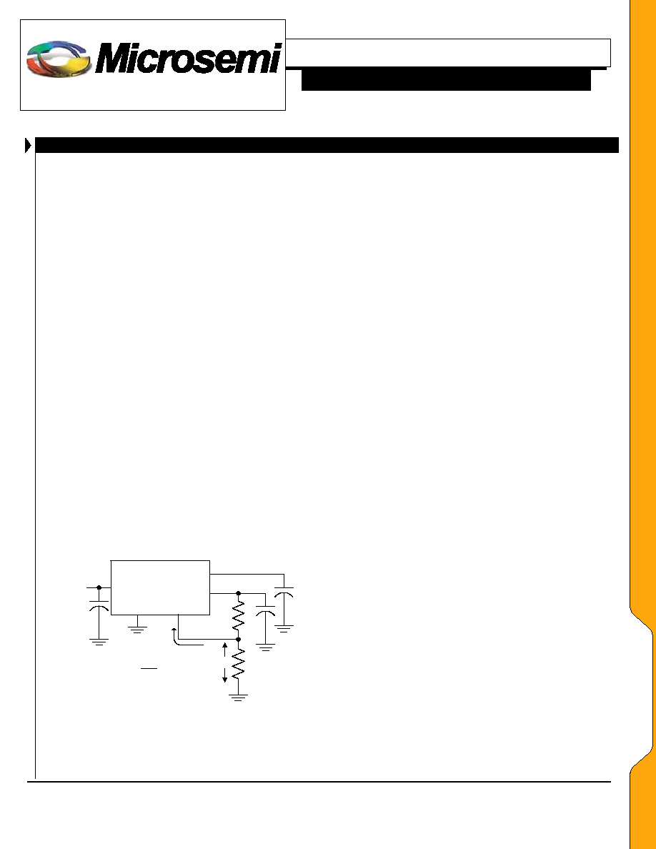
Adjustable Output Voltage
The LX8816 develops a 1.25V reference voltage between the adjust
terminal and GND (See Figure 2). By placing a resistor, R2, between
these two terminals, a constant current is caused to flow through R1
and down through R2 to set the overall output voltage. Because I
ADJ
is
very small and constant when compared with the current through R2, it
represents a small error and can usually be ignored.
LX8816-04
R1
R2
V
IN
ADJ
V
1
FIGURE 2 - BASIC ADJUSTABLE
REGULATOR
V
REF
1
2
1
1
1
R
I
R
R
V
V
ADJ
REF
+
+
=
I
ADJ
1µA
V
2
Minimum Load Requirement
The LX8816 has a minimum load is requirement for proper output
regulation. This minimum current is specified at 0mA for the fixed
output and 2ma for the adjustable output regulators.
Temperature Protection
The thermal protection shuts the LX8816 down when the junction
temperature exceeds 140
0
C. Each output has independent thermal
shutdown capability. Exposure to absolute maximum rated conditions
for extended periods may affect device reliability, see Thermal
Considerations below.
Current Limit Protection
The LX8816 includes over current protection, when the output load
current exceeds typically 1.4A the circuit forces the regulator decrease
in output.
Thermal Considerations
Thermal shutdown protects the integrated circuit from thermal
overload caused from a rise in junction temperature during power
dissipation. This means of protection is intended for fault protection
only and not as a means of current or power limiting during normal
application usage. Proper thermal evaluation should be done to ensure
that the junction temperature dose not exceed it's maximum rating.
Operating at the maximum T
J
of 150∞C can impact reliability . Due to
variation in individual device electrical characteristics and thermal
resistance , the built in thermal overload protection may be activated at
power levels slightly above or below the rated dissipation. Also peak
output power should be considered for each individual output.
Power dissipation for regulator can be calculated using the following
equation:
P
D
= (V
IN(MAX)
-V
1
) * I
1
+
(V
IN(MAX)
-V
2
) * I
2
(Note: power dissipation resulting from quiescent (ground) current is negligible)
For the S-PAK package, thermal resistance,
TAB-AMB
is 25-45
0
C/W
depending on mounting technique when mounted on a FR4 copper
clad PCB. Junction temperature of the integrated circuit can be
calculated using:
T
JUNCTION
= T
JUNCTION-TAB RISE _
+ T
TAB-AMB RISE
+
T
AMB
T
TAB
= P
D MAX
*
JT ;
T
TAB-AMB
= (P
D REG1
+ P
D REG2
) *
PCB
An example: Given conditions: T
A
= 50∞C, V
IN
= 5.0V, V
1
= 2.5V, I
1
=
210mA, V
2
= 3.3V I
2
= 1A.
Calculated values:
T
J-TAB REG1
= (5V-2.5V) * (210mA) * 4.5∞C/W = (0.525) * 4.5∞C/W = 2.4∞C
T
J-TAB REG2
= (5V-3.3V) * (1.0A) * 4.5∞C/W = (1.7) * 4.5∞C/W = 7.7∞C
T
TAB-AMB RISE
= ( 0.525W + 1.7W ) * 30∞C/W = 66.8∞C
T
JUNCTION
=
10.1∞C + 66.8∞C +
5
0∞C = 126.9∞C
It is important to note that although each output of the regulator will
produce up to 1A in current, the individual or total power dissipation
may limit the useful total current draw. The junction temperature
should be calculated for each individual output as well as the
combined outputs to insure the maximum junction temperature in not
exceeded.
A
A
P
P
P
P
L
L
I
I
C
C
A
A
T
T
I
I
O
O
N
N
Microsemi
Integrated Products
11861 Western Avenue, Garden Grove, CA. 92841, 714-898-8121, Fax: 714-893-2570
Page 7
Copyright
2000
Rev. 1.2a, 2002-11-01
WWW
.
Microse
m
i
.
CO
M
LX8816
Dual Channel 1A Low Dropout Regulator
P
RODUCTION
D
ATA
S
HEET
I N T E G R A T E D P R O D U C T S
A P P L I C A T I O N I N F O R M A T I O N
Layout Consideration
The layout must be done with low impedance paths for V
IN
, V
1,
V
2
and
Ground by using sufficiently wide traces to avoid voltage drops and
noise pick up. The output capacitors must be placed as close as
possible to the voltage regulator output pins. To allow the same
voltage reference for all circuits, use a star configuration from the
output capacitors to the different loads. The input capacitor should be
connected between V
IN
and ground with short leads. Although it may
not be immediately obvious, best load regulation for the adjustable
output is obtained when the top of the resistor divider, (R1), is
connected as close as possible to the case of the regulator, not to the
load.
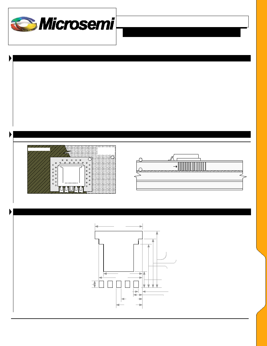
Heatsink Consideration
The PCB copper can be used as a heatsink for the surface mounted
S-Pak. Using the minimum size as shown in the recommended pad
layout limits the usable power to about 1W for ambient temperature of
50∞C. Since most applications require greater than 2W there is the
need to provide additional heat sinking. This can be accomplished by
using additional copper area both on the PCB surface as shown in the
possible heat sink layout below, or to an embedded ground plane.
Since the die pad (copper tab) is in electrical contact with ground, the
designer can use thermal vias on the surface of the PCB taking
advantage of the heat-spreading (Cu) layer of an internal ground plane.
H E A T S I N K L A Y O U T
B oard Level
G round
P lane
C om ponent
Trace
B
A
Component
Component Trace
Ground Plane
Inner Power Plane
Backside Trace
VIAS
B
A
Figure 3 - Heatsink
R E C O M M E N D E D M I N I M U M P C B F O O T P R I N T
11.56mm
9.98mm
8.84mm
3.28mm
.86mm
1.83mm
4.39mm
5.36mm
7.92mm
9.75mm
8.89mm
0mm
1.37mm
A
A
P
P
P
P
L
L
I
I
C
C
A
A
T
T
I
I
O
O
N
N
Microsemi
Integrated Products
11861 Western Avenue, Garden Grove, CA. 92841, 714-898-8121, Fax: 714-893-2570
Page 8
Copyright
2000
Rev. 1.2a, 2002-11-01
WWW
.
Microse
m
i
.
CO
M
LX8816
Dual Channel 1A Low Dropout Regulator
P
RODUCTION
D
ATA
S
HEET
I N T E G R A T E D P R O D U C T S
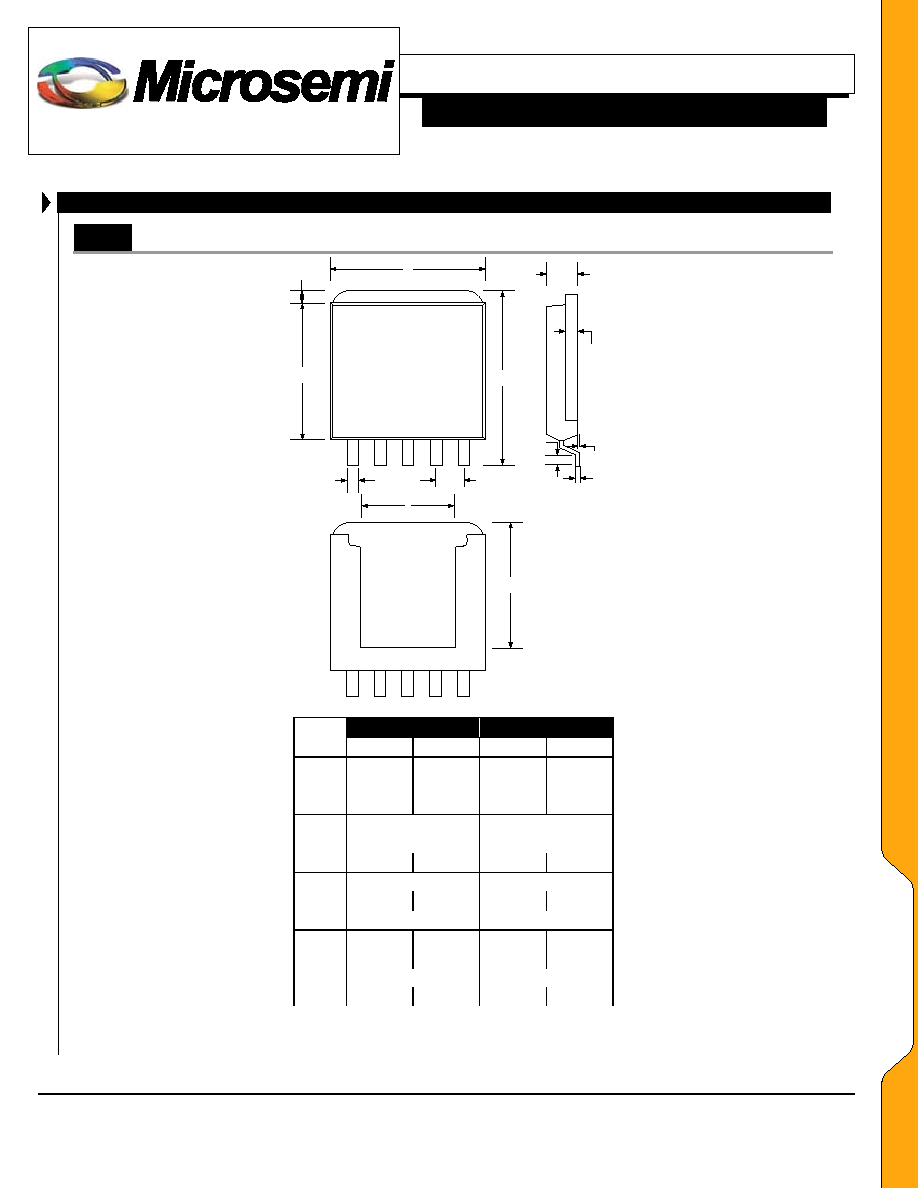
P A C K A G E D I M E N S I O N S
DF
5-Pin Plastic S-Pak
A
B
K
F
G
J
H
C
E
I
D
L
M
M
ILLIMETERS
I
NCHES
Dim
MIN MAX MIN MAX
A 9.27 9.52 0.365
0.375
B 7.87 8.13 0.310
0.320
C 1.78 2.03 0.070
0.080
D
8.03 BSC
0.316 BSC
E
0.25 BSC
0.010 BSC
F 0.63 0.79 0.025
0.031
G
1.70 BSC
0.067 BSC
H 0.79 1.04 0.031
0.041
I
6.50 BSC
0.256 BSC
J 0.03 0.13
0.001
0.005
K 10.41 10.67 0.410 0.420
L
0.25 BSC
0.01 BSC
M 0.76 1.27 0.03 0.05
Note:
Dimensions do not include mold flash or protrusions; these shall not exceed 0.155mm(.006") on any side. Lead dimension shall not
include solder coverage.
M
M
E
E
C
C
H
H
A
A
N
N
I
I
C
C
A
A
L
L
S
S
Microsemi
Integrated Products
11861 Western Avenue, Garden Grove, CA. 92841, 714-898-8121, Fax: 714-893-2570
Page 9
Copyright
2000
Rev. 1.2a, 2002-11-01
WWW
.
Microse
m
i
.
CO
M
LX8816
Dual Channel 1A Low Dropout Regulator
P
RODUCTION
D
ATA
S
HEET
I N T E G R A T E D P R O D U C T S
N O T E S
PRODUCTION DATA ≠ Information contained in this document is proprietary to
Microsemi and is current as of publication date. This document may not be modified in
any way without the express written consent of Microsemi. Product processing does not
necessarily include testing of all parameters. Microsemi reserves the right to change the
configuration and performance of the product and to discontinue product at any time.
N
N
O
O
T
T
E
E
S
S
KD
Digitally
signed by
KD
DN:
cn=KD,
o=Microse
mi, c=US
Date:
2002.11.01
10:07:28
-08'00'
Signat
ure
invalid