 | –≠–ª–µ–∫—Ç—Ä–æ–Ω–Ω—ã–π –∫–æ–º–ø–æ–Ω–µ–Ω—Ç: LX8821 | –°–∫–∞—á–∞—Ç—å:  PDF PDF  ZIP ZIP |
P
RODUCTION DATA
S
HEET
Microsemi
Microsemi Microelectronics Division
11861 Western Avenue, Garden Grove, CA. 92841, 714-898-8121, Fax: 714-893-2570
Page 1
Copyright
© 2005
Rev. 1.1, 2005-03-09
WWW
.
Microse
m
i
.
CO
M
LX8821
D
UAL
C
HANNEL
2.5A
L
OW
D
ROPOUT
R
EGULATOR
TM
Æ
D E S C R I P T I O N
The LX8821 is a positive-voltage
linear regulator with one fixed and
one adjustable output featuring low-
dropout and high accuracy.
To maximize efficiency, the
LX8821 accepts two supply voltage
inputs for the V
CONTROL
and V
POWER
sections. This configuration reduces
power dissipation by operating the
regulator near dropout (V
PWR
-V
OUT
=
VDO = 0.4V @ 2A) while providing
sufficient operating headroom for the
control logic.
Each channel can supply up to
2.5A independently with a regulator
design optimized for system
efficiency by consuming minimal
ground current and directing
quiescent current to the load
The internal voltage reference is
trimmed at wafer level, enabling
precise output voltages, typically
±1% of its specified value.
Power sequencing logic ensures
proper startup regardless of the
level of V
CTRL
or V
PWR
. The
LX8821 outputs remain off while
V
PWR
< 2.2V.
Thermal and Short Circuit
Current Protection are integrated
on-chip and operate independently
for each regulator output.
The LX8821 regulator is stable
with a wide range of output
capacitance and ESR; typically
10
F tantalum or ceramic on the
outputs is sufficient.
Microsemi uses a low profile
power package with low thermal
resistance and ease of assembly
using surface mount technology.
IMPORTANT: For the most current data, consult Microsemi's website: http://www.microsemi.com
K E Y F E A T U R E S
Two Independent Regulated
Outputs
Wide DC Supply Voltage of 3.0V to
10.0V
Accurate Output Voltages
Low Tolerance Line (0.5%) and
Load (0.5%) Regulation
Max. Dropout of 0.6V at Rated
Current
Independent Thermal and Current
Limit Protection
Loop Stability Independent of
Output Capacitor
Type SMT Power Package
A P P L I C A T I O N S / B E N E F I T S
ASIC, Memory, I/O
Low Voltage Logic Supplies
Active SCSI Terminators
Battery Charging Circuits
PC Peripherals
Instrumentation
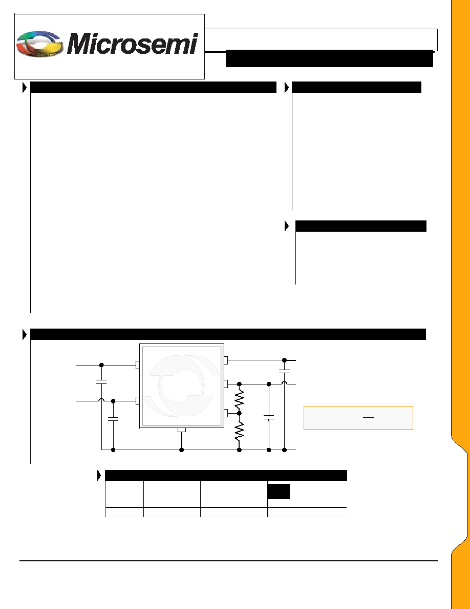
P R O D U C T H I G H L I G H T
Part
V
PWR
V
CONTROL
GND
ADJ
V
OUT2
V
OUT1
V
POWER
10µF
V
CONTROL
1µF
R2
R1
33µF
33µF
GROUND
V
OUT2
V
OUT1
LX8821
R1
I
R2
R1
1
1.25
V
ADJ
OUT2
∑
+
+
∑
=
P A C K A G E O R D E R I N F O
DF
Plastic
S-Pak
7-Pin
T
A
(
∞C)
Output V1
Output V2
RoHS Compliant
0 to 100
1.5V
Adjustable
LX8821CDF
Note: Available in Tape & Reel. Append the letters "TR" to the part number. (i.e. LX8821CDF-TR)
L
L
X
X
8
8
8
8
2
2
1
1
P
RODUCTION DATA
S
HEET
Microsemi
Microsemi Microelectronics Division
11861 Western Avenue, Garden Grove, CA. 92841, 714-898-8121, Fax: 714-893-2570
Page 2
Copyright
© 2005
Rev. 1.1, 2005-03-09
WWW
.
Microse
m
i
.
CO
M
LX8821
D
UAL
C
HANNEL
2.5A
L
OW
D
ROPOUT
R
EGULATOR
TM
Æ
A B S O L U T E M A X I M U M R A T I N G S
Input
Voltage
(V
CTRL
, V
PWR
).........................................................................13.5V
Load Current (Internally Limited) ..................................................................3.0A
Power Dissipation ......................................................................Internally Limited
Short-Circuit Protection .......................................................................... Indefinite
Operating Junction Temperature.................................................................. 150
∞C
Storage Temperature Range...........................................................-65
∞C to 150∞C
Peak Package Solder Reflow Temperature
(40 second maximum exposure) ..................................................... 260∞C (+0, -5)
Note: Exceeding these ratings could cause damage to the device. All voltages are with respect to
Ground. Currents are positive into, negative out of specified terminal
.
T H E R M A L D A T A
DF
Plastic S-Pak 7-Pin
THERMAL RESISTANCE
-
JUNCTION TO
T
AB
,
JT
4.5
∞
C/W
THERMAL RESISTANCE
-
JUNCTION TO
A
MBIENT
,
JA
20 - 50
∞
C/W
Junction Temperature Calculation: T
J
= T
A
+ (P
D
x
JA
).
The
JA
numbers are guidelines for the thermal performance of the device/pc-board system.
All of the above assume no ambient airflow.
JA
can vary from 10
∞C/W to > 50∞C/W
depending on mounting technique. (See Application Notes Section: Thermal considerations)
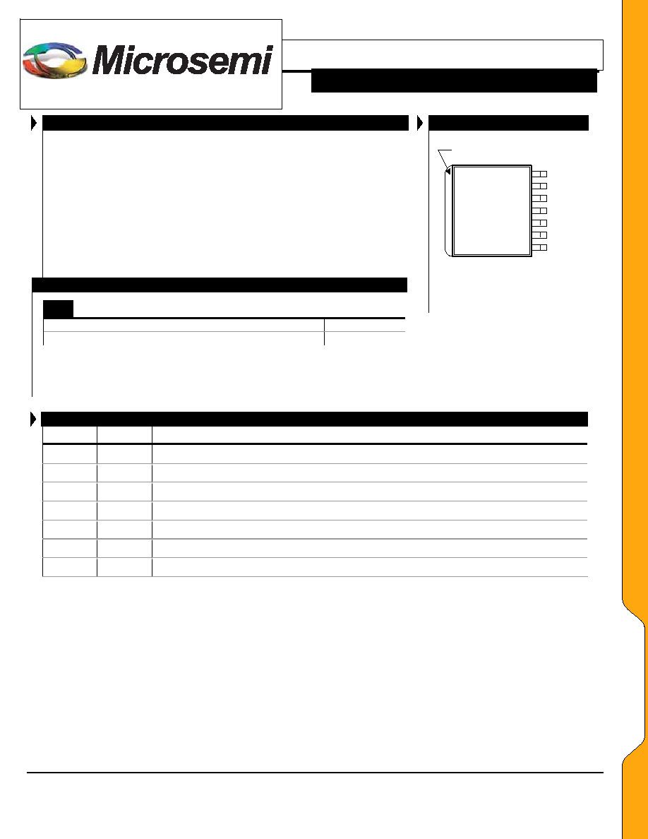
PACKAGE PIN OUT
DF P
ACKAGE
(Top View)
1
V
CTRL
V
OUT1
V
PW R
GND
V
OUT2
2
3
4
5
TAB is GND
ADJ
V2
6
NC
7
Pin 4 and Tab are common
RoHS 100% Matte Tin Lead Finish
F U N C T I O N A L P I N D E S C R I P T I O N
P
IN
N
AME
D
ESCRIPTION
1 V
CTRL
Unregulated input voltage supply, provides bias for control circuitry, (V
CTRL
≠ V
OUT
) > 1V.
2 V
OUT1
Regulator #1 fixed output voltage, 1.5V nominal.
3 V
PWR
Unregulated input voltage supply for power section. For proper operation: (V
PWR
≠ V
OUT
) > V
DROPOUT
.
4
GND
Common terminal for ground reference, Tab of package is internally connected to this pin.
5 V
OUT2
Regulator #2 output
6 ADJ
V2
Regulator #2 feedback voltage, servos to 1.25V. Using external resistors to program V
OUT2
.
7
---
Not used, no internal connection, may be left floating or connected to any other pin or voltage.
P
P
A
A
C
C
K
K
A
A
G
G
E
E
D
D
A
A
T
T
A
A
P
RODUCTION DATA
S
HEET
Microsemi
Microsemi Microelectronics Division
11861 Western Avenue, Garden Grove, CA. 92841, 714-898-8121, Fax: 714-893-2570
Page 3
Copyright
© 2005
Rev. 1.1, 2005-03-09
WWW
.
Microse
m
i
.
CO
M
LX8821
D
UAL
C
HANNEL
2.5A
L
OW
D
ROPOUT
R
EGULATOR
TM
Æ
E L E C T R I C A L C H A R A C T E R I S T I C S
Unless otherwise specified, the following specifications apply over the operating ambient temperature 0
∞C
T
A
100
∞C except where
otherwise noted and the following test conditions: V
CTRL
= 5V, V
PWR
= 3.3V I
OUT
= 5mA, C
1, 2, 3, 4
= 10
F (Tantalum), and T
J
= T
A
using
low duty cycling methods. Typical values represent performance @ 23∞C
LX8821
Parameter Symbol
Test
Conditions
Min Typ Max
Units
FIXED OUTPUT: V
OUT 1
Total Output Voltage Variation
V
1
5mA < I
1
< 2.5A, 3.75V < V
CTRL
< 8V
3.3V < V
PWR
< 5.5V
1.455 1.500 1.545 V
Line
Regulation
V
1
(V
IN
)
3.3V<V
CTRL
<10V, 3.3V<V
PWR
<5.5V, I
1
= 5mA
1
5
mV
Load
Regulation
V
1
(I
1
)
5mA < I
1
< 2.5A, V
CTRL
=5V, V
PWR
=3.3V
1
5
mV
Current
Limit
I
1 (MAX)
2.55
3.0
A
Minimum Load Current
I
1
Note 1
0
5
mA
ADJUSTABLEOUTPUT: V
OUT 2
5mA < I
2
< 2.5A, 3.75V < V
CTRL
< 8V
2.97V < V
PWR
< 3.63V
1.225 1.25 1.275
Output
Voltage
V
2
5mA < I
2
< 2.5A, 3.75V < V
CTRL
< 8V,
3.3V < V
PWR
< 5.5V
1.225 1.25 1.288
V
Line
Regulation
V
2
(V
IN
)
3.3V<V
CTRL
<10V, 3.3V<V
PWR
<5.5V, I
2
= 5mA
0.5
5
mV
Load
Regulation
V
2
(I
2
)
5mA < I
2
< 2.5A, V
CTRL
=5V, V
PWR
=3.3V
8
20
mV
I
OUT
= 2.5A, V
O
= -2%
0.500
0.750
I
OUT
= 2.0A, V
O
= -2%
0.413
0.600
V
PWR
-V
2
I
OUT
= 1.0A, V
O
= -2%
0.167
0.400
V
I
OUT
= 2.5A, V
O
= -2%
0.95
1.10
Dropout Voltage, V
OUT 2
V
CNTR
-V
2
I
OUT
= 1.0A, V
O
= -2%
0.80
1.00
V
Adjust Pin Current
I
1
= I
2
= 5mA, T
J
= 25∞C
0.2
1
µA
Current
Limit
I
2 (MAX)
2.55
3.0
A
Minimum Load Current
I
2
Note 1
1
5
mA
ENTIRE REGULATOR
V
PWR
2.6 V
Minimum Operating Voltage
V
CONTROL
3.3
V
Under
Voltage
Lockout
V
PWR
Rising, 3.0V<V
CTRL
< 10V, Both Outputs
Guaranteed Off
2.2
V
I
1
=I
2
=5mA
3
5
mA
Quiescent Current
I
Q
I1 = I2 = 2.5A
5
10
mA
Ripple
Rejection
PSRR f=120Hz, T
J
= 25
∞C
60 75 dB
RMS Output Noise
10Hz < f < 10kHz
0.003
%V
OUT
Thermal
Shutdown
T
JSD
160
∞C
Note 1: Minimum load current is defined as the amount of output current required to maintain regulation
E
E
L
L
E
E
C
C
T
T
R
R
I
I
C
C
A
A
L
L
S
S

P
RODUCTION DATA
S
HEET
Microsemi
Microsemi Microelectronics Division
11861 Western Avenue, Garden Grove, CA. 92841, 714-898-8121, Fax: 714-893-2570
Page 4
Copyright
© 2005
Rev. 1.1, 2005-03-09
WWW
.
Microse
m
i
.
CO
M
LX8821
D
UAL
C
HANNEL
2.5A
L
OW
D
ROPOUT
R
EGULATOR
TM
Æ
C H A R A C T E R I S T I C C U R V E R S
V
OUT
Error vs. Temperature
-0.025%
0.000%
0.025%
0.050%
0.075%
0.100%
0.125%
0.150%
0.175%
0.200%
0
25
50
75
100
125
Temp, ∞C
E
rro
r V
o
l
t
a
g
e
Vo2
Vo1
Dropout Voltage
0.05
0.10
0.15
0.20
0.25
0.30
0.35
0.40
0.45
0.50
0.55
0.60
0.65
0.70
-50
-25
0
25
50
75
100
125
150
Tem perature (∞C)
VD
D
(
V
)
Iout=2.5A
Iout=1A
Iout=0.5A
Quiescent Current
0
1
2
3
4
5
6
7
8
-5
0
-2
5
0
25
50
75
100
125
150
Tem perature (∞C)
I
G
R
O
UN
D (
m
A
)
IL1&IL2=5mA
IL1&IL2=2.5A
Power On Ramp: Supply Ramp
CH4
1
2
3
4
2.00V
1.00V
2.00V
2.00V
1.00ms
CH1 800mV
CH1
CH3
M
A
B
W
B
W
CH2
CH1
=
V
P
= V
C
CH3 = V
O2
CH2
=
V
O1
CH4 = I
P
2A/DIV
Step Load Response With Ceramic Cap (10µF)
CH1 = V
O1
, CH2 = V02
,
CH4 = I
O1
(50mA to 0.55A Step)
Step Load Response With Tantalum Cap (10µF)
CH1 = V
O1
, CH2 = V02
,
CH4 = I
O1
(50mA to 0.55A Step)
G
G
R
R
A
A
P
P
H
H
S
S
P
RODUCTION DATA
S
HEET
Microsemi
Microsemi Microelectronics Division
11861 Western Avenue, Garden Grove, CA. 92841, 714-898-8121, Fax: 714-893-2570
Page 5
Copyright
© 2005
Rev. 1.1, 2005-03-09
WWW
.
Microse
m
i
.
CO
M
LX8821
D
UAL
C
HANNEL
2.5A
L
OW
D
ROPOUT
R
EGULATOR
TM
Æ
A P P L I C A T I O N I N F O R M A T I O N
The LX8821 is part of a family of Dual LDO (Low Drop-Out)
linear regulators in Microsemi's S-PAK power package which offer
maximum power dissipation in a low profile surface mount
technology. The family includes combination fixed and adjustable
versions. Each channel can supply up to 2.5A independently with a
regulator design optimized for system efficiency by consuming
minimal ground current and directing quiescent current to the load.
INPUT CAPACITOR
To improve load transient response and noise rejection an input
bypass capacitor is of at least 10µF is required. Generally we
recommend a 10µF ceramic or tantalum or 22µF electrolytic
capacitor.
OUTPUT CAPACITOR
The regulator requires output capacitors connected between each
output (V1, V2) to GND to stabilize the internal control loop. Many
types of capacitors are available, with different capacitance values
tolerances, temperature coefficients and equivalent series resistance.
We recommend a minimum of 10µF. To ensure good transient
response from the power supply system under rapidly changing
current load conditions, designers generally use additional output
capacitors connected in parallel. Such an arrangement serves to
minimize the effects of the parasitic resistance (ESR) and
inductance (ESL) that are present in all capacitors. The regulator
has been tested stable with capacitor ESR's in the range of 0.05 to 2
ohms. We have found it best to use the same type of capacitor for
both input and output bypass.
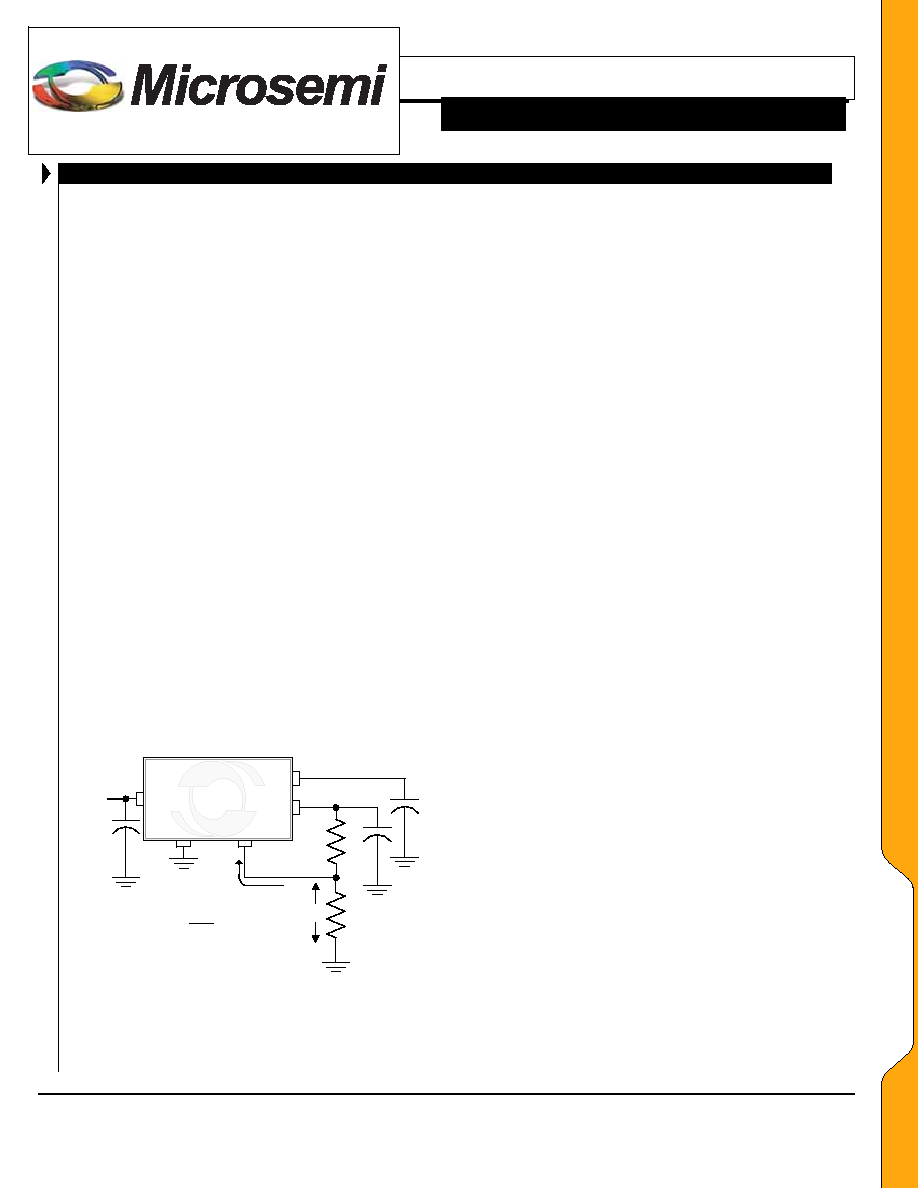
ADJUSTABLE OUTPUT VOLTAGE
The LX8821 develops a 1.25V reference voltage between the
adjust terminal and GND (See Figure 2). By placing a resistor, R2,
between these two terminals, a constant current is caused to flow
through R1 and down through R2 to set the overall output voltage.
Because I
ADJ
is very small and constant when compared with the
current through R2, it represents a small error and can usually be
ignored.
R1
R2
V
IN
ADJ
V
2
V
REF
1
2
1
1
2
R
I
R
R
V
V
ADJ
REF
+
+
=
I
ADJ
1µA
V
1
Part
LX8821
Figure 2 ≠
Basic Adjustable Regulator
MINIMUM LOAD REQUIREMENT
The LX8821 has a minimum load requirement for proper output
regulation. This typical current is specified at 0mA for the fixed
output and 1ma for the adjustable output regulators.
TEMPERATURE PROTECTION
The thermal protection shuts the LX8821 down when the junction
temperature exceeds 160∞C. Each output has independent thermal
shutdown capability. Exposure to absolute maximum rated
conditions for extended periods may affect device reliability: see
Thermal Considerations below.
CURRENT LIMIT PROTECTION
The LX8821 includes over current protection; when the output
load current exceeds typically 3A the circuit forces the regulator
decrease in output.
THERMAL CONSIDERATIONS
Thermal shutdown protects the integrated circuit from thermal
overload caused from a rise in junction temperature during power
dissipation. This means of protection is intended for fault protection
only and not as a means of current or power limiting during normal
application usage. Proper thermal evaluation should be done to
ensure that the junction temperature dose not exceed it's maximum
rating. Operating at the maximum T
J
of 150∞C can impact
reliability. Due to variation in individual device electrical
characteristics and thermal resistance, the built in thermal overload
protection may be activated at power levels slightly above or below
the rated dissipation. Also peak output power should be considered
for each individual output.
Power dissipation for regulator can be calculated using the
following equation:
2
2
IN(MAX)
1
1
IN(MAX)
D
I
)
V
(V
I
)
V
(V
P
◊
-
+
◊
-
=
(Note: power dissipation resulting from quiescent (ground) current
is negligible)
Thermal resistance,
TAB-AMB
ranges from 25-45
0
C/W depending
on mounting technique using a FR4 copper clad PCB. Junction
temperature of the integrated circuit can be calculated using:
AMB
AMB
TAB
TAB
JUNCTION
JUNCTION
T
T
T
T
+
+
=
-
-
JT
DMAX
TAB
P
T
◊
=
;
PCB
2
DREG
1
DREG
AMB
TAB
)
P
(P
T
◊
+
=
-
An example: Given conditions: T
A
= 50∞C, V
IN
= 5.0V, V
1
= 1.5V,
I
1
= 210mA, V
2
= 3.3V I
2
= 1A.
Calculated values:
C
3.3
C/W
4.5
(0.735)
C/W
4.5
(0.21A)
1.5V)
(5V
T
REG1
TAB
J
∞
=
∞
◊
=
∞
◊
◊
-
=
-
C
C/W
C/W
V
V
7.7
4.5
(1.7)
4.5
(1A)
)
3.3
(5
T
REG2
TAB
J
∞
=
∞
◊
=
∞
◊
◊
-
=
-
C
73.1
C/W
30
1.7W)
(0.735W
T
AMB
TAB
∞
=
∞
◊
+
=
-
C
130.8
C
50
C
73.1
C
7.7
T
MAX
-
JUNCTION
∞
=
∞
+
∞
+
∞
=
It is important to note that although each output of the regulator
will produce up to 2.5A in current, the individual or total power
dissipation may limit the useful total current draw. The junction
temperature should be calculated for each individual output as well
as the combined outputs to insure the maximum junction
temperature is not exceeded.
A
A
P
P
P
P
L
L
I
I
C
C
A
A
T
T
I
I
O
O
N
N
S
S
P
RODUCTION DATA
S
HEET
Microsemi
Microsemi Microelectronics Division
11861 Western Avenue, Garden Grove, CA. 92841, 714-898-8121, Fax: 714-893-2570
Page 6
Copyright
© 2005
Rev. 1.1, 2005-03-09
WWW
.
Microse
m
i
.
CO
M
LX8821
D
UAL
C
HANNEL
2.5A
L
OW
D
ROPOUT
R
EGULATOR
TM
Æ
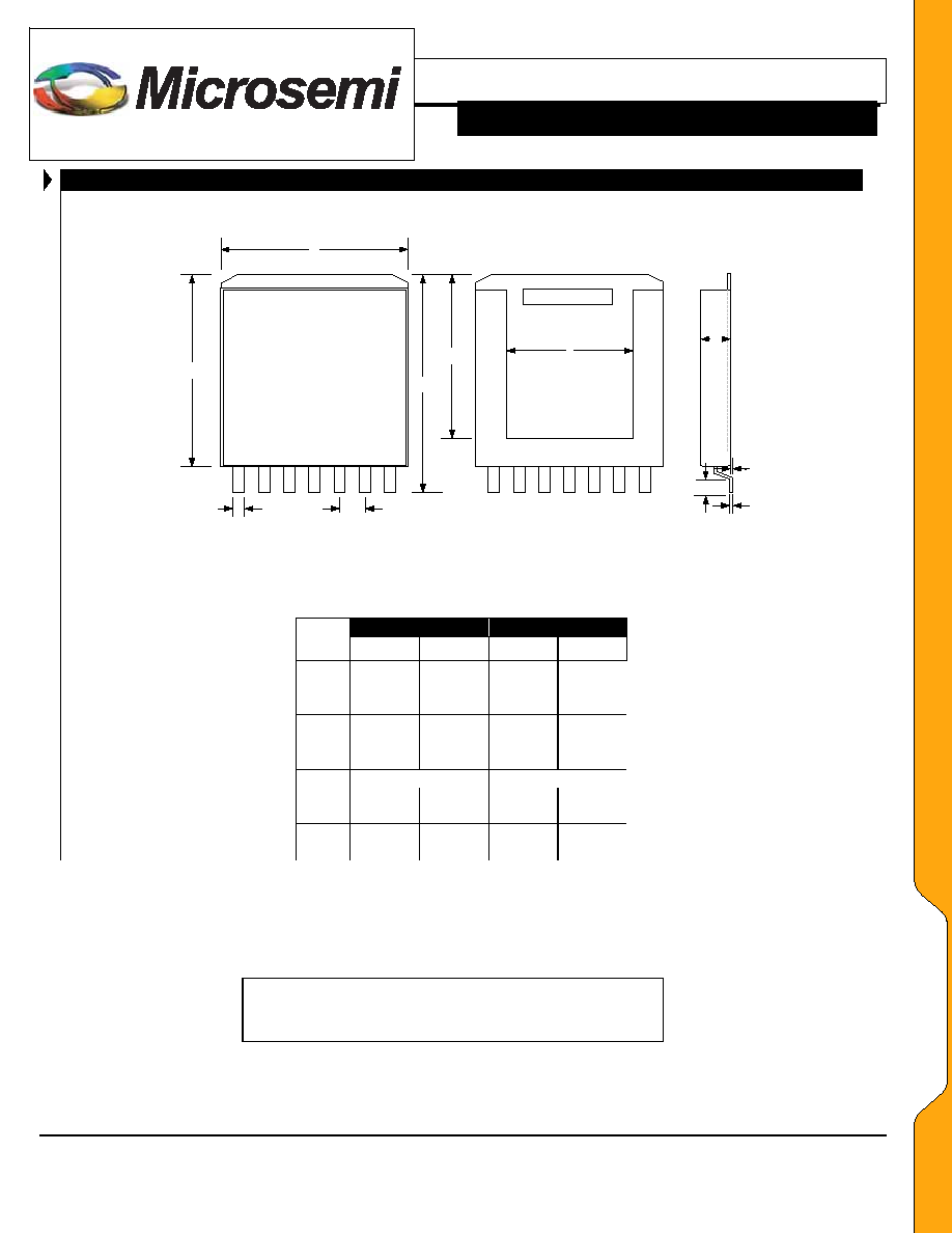
M E C H A N I C A L D I M I N E S I O N S
A
B
K
F
G
I
D
C
H
J
E
Note:
1. Dimensions do not include mold flash or protrusions; these shall not exceed 0.155mm(.006") on any side. Lead
dimension shall not include solder coverage
M
ILLIMETERS
I
NCHES
Dim
MIN MAX MIN MAX
A 9.27 9.52 .365 .375
B 8.89 9.14 .350 .360
C 1.77 2.03 .070 .080
D 7.49 7.74 .295 .305
E 0.12 0.38 .005 .015
F 0.58 0.84 .023 .033
G
1.27 BSC
0.050 BSC
H 0.79 1.04 .031 .041
I 4.31 6.86 .170 .270
J 0.03 0.13 .001 .005
K 10.41 10.67 .410 .420
PRODUCTION DATA ≠ Information contained in this document is proprietary to
Microsemi and is current as of publication date. This document may not be modified in
any way without the express written consent of Microsemi. Product processing does not
necessarily include testing of all parameters. Microsemi reserves the right to change the
configuration and performance of the product and to discontinue product at any time.
M
M
E
E
C
C
H
H
A
A
N
N
I
I
C
C
A
A
L
L
S
S