D E S C R I P T I O N
lation, lamp current regulation, and lamp
dimming in a single power stage made up
of two pairs of low loss FET's. The FET's
drive an LC resonant circuit that feeds the
primary of a high voltage transformer with
a sinusoidal voltage.
Required L and C values in the resonant
circuit are such that very low loss compo-
nents can be used to obtain higher electri-
cal efficiency than is possible with previous
topologies.
The full bridge LXM1597-01 is optimized
to efficiently operate with up to 4 watt lamps
at input voltages of 5 volts. This module
will operate over the full 4.5V to 7V input
voltage range.
The modules are equipped with a dim-
ming input that permits full range bright-
ness control from an external potentiom-
eter, and a sleep input that reduces module
power to a few microwatts in shut down
mode.
All modules feature output open and short
circuit protection.
LXM1597-01 CCFL (cold cathode florescent
lamp) Inverter Modules are specifically de-
signed for driving LCD back light lamps in
applications where dimmability, ultra-high
efficiency, high light output, low noise emis-
sions, reliable fail safe design, and small form
factors are critical parameters. Both mono-
chrome and color displays are supported.
The modules convert unregulated DC
voltage from the system battery or AC
adapter directly to high-frequency, high-
voltage sine waves required to ignite and
operate CCFL lamps. The module design is
based on a proprietary Linfinity IC that pro-
vides important new performance advances.
Remarkable improvements in efficiency
and RF emissions result from its single stage
resonant inverter featuring a patent pend-
ing Current Synchronous, Zero Voltage
Switching (CS-ZVS) topology. CS-ZVS pro-
duces nearly pure sine wave currents in the
lamp enabling maximum light delivery while
reducing both conducted and radiated noise.
This topology simultaneously performs
three tasks consisting of line voltage regu-
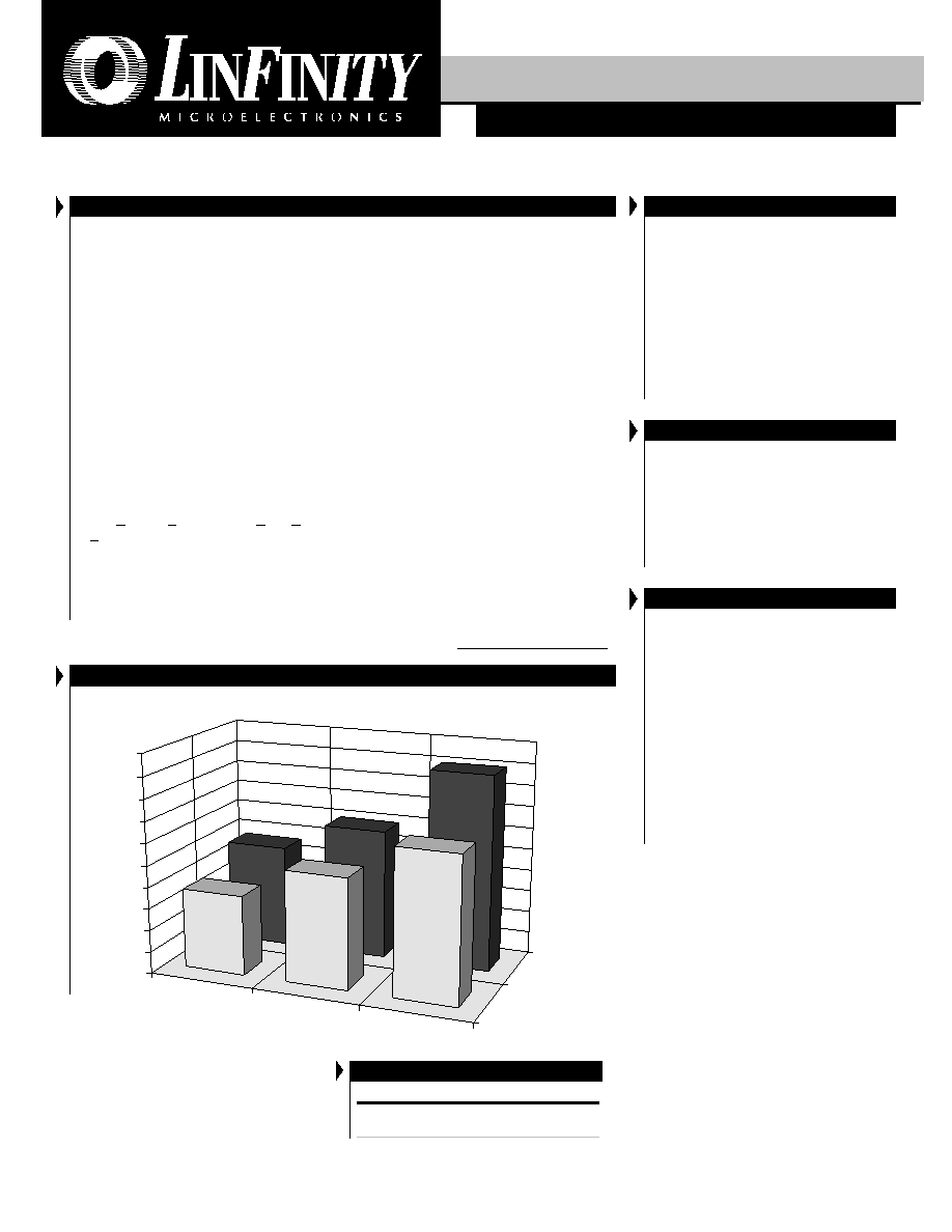
P R O D U C T H I G H L I G H T
B
A C K L I G H T
I
N V E R T E R
L
I G H T
O
U T P U T
E
F F I C I E N C Y
C
O M P A R I S O N
Computer 1
Computer 2
Computer 3
Stock
Linfinity
0
5
10
15
20
25
30
35
40
45
50
Eff (Nits / Watts)
5 V C C F L I
N V E R T E R
M
O D U L E S
Not recommended for New Designs
T
H E
I
N F I N I T E
P
O W E R
O F
I
N N O V A T I O N
LXM1597-01
LIN D
O C
#: 1597
P
A T E N T
P
E N D I N G
K E Y F E A T U R E S
s 15 to 30% More Light Output
s Closed Loop, Fully Regulating Design
s 4.5V To 7V Input Voltage Range
s Versatile Brightness Control Input
s 3 MicroAMP Sleep Current
s Output Short Circuit Protection And
Automatic Over-Voltage Limiting
s 8mm Max. Height, Narrow Footprints
s Single Sided PCB Is Self Insulating
A P P L I C A T I O N S
s
s
s
s
s Notebook And Sub-Notebook Computers
s Personal Digital Assistants
s Portable Instrumentation
s Automotive Displays
s Desktop Displays
s Airline Entertainment Centers
B E N E F I T S
s Ultra-High Efficiency, Line Voltage
Regulation And Sleep Mode Extend
Computer Battery Life
s Cool Operation PermitS Close Proximity
To LCD Panel Without Display Distortion
s Smooth, Full-Range Brightness Control
Gives Your Product A High Quality Image
s Low EMI / RFI Design Minimizes Shielding
Requirements
s Narrow, Low-Profile Standard Modules Fit
Into Most LCD Enclosures
s Single Sided PCB Saves Expensive High
Voltage Insulating Tapes
Copyright © 1998
Rev. 0.6a 10/00
1
11861 W
ESTERN
A
VENUE
, G
ARDEN
G
ROVE
, CA. 92841, 714-898-8121, F
AX
: 714-893-2570
L
I N
F
I N I T Y
M
I C R O E L E C T R O N I C S
I
N C
.
IMPORTANT: For the most current data, consult LinFinity's web site: http://www.linfinity.com.
LXM1597-01
5V I N P U T
M O D U L E O R D E R I N F O
5 V C C F L I
N V E R T E R
M
O D U L E S
LXM1597-01
P R O D U C T D A T A B O O K 1 9 9 6 / 1 9 9 7
Copyright © 1998
Rev. 0.6a 10/00
2
Not Recommended for New Designs
P
A T E N T
P
E N D I N G
A B S O L U T E M A X I M U M R AT I N G S
( N o t e 1 )
Input Supply Voltage (V
IN
) ............................................................................................................................................................................... -0.3V to 7.0V
Output Voltage, no load ........................................................................................................................................................ Internally Limited to 1900V
RMS
Output Current ......................................................................................................................................................................... 8.0mA
RMS
(Internally Limited)
Output Power .................................................................................................................................................................................................................. 4.2W
Input Signal Voltage, (SLEEP and BRITE Inputs) ............................................................................................................................................ -0.3V to 6.5V
Ambient Operating Temperature, zero airflow .................................................................................................................................................. 0∞C to 60∞C
Storage Temperature Range .............................................................................................................................................................................. -40∞C to 85∞C
Note 1.
Exceeding these ratings could cause damage to the device. All voltages are with respect to Ground. Currents are positive into, negative out of
the specified terminal.
R E C O M M E N D E D O P E R A T I N G C O N D I T I O N S (R.C.)
This module has been designed to operate over a wide range of input and output conditions. However, best efficiency and performance
will be obtained if the module is operated under the condition listed in the 'R.C.' column. Min. and Max. columns indicate values beyond
which the inverter, although operational, will not function optimally.
Input Supply Voltage
V
IN
Output Power
P
O
Brightness Control Input Voltage Range
V
BRITE
Lamp Operating Voltage
V
LAMP
Lamp Current - Full Brightness
I
OLAMP
Operating Ambient Temperature Range
T
A
Parameter
Symbol
Units
Recommended Operating Conditions
Min.
R.C.
Max.
4.5
5
7
V
2.5
4.0
W
0.8
2.5
V
240
500
650
V
RMS
5
7
mA
RMS
0
60
∞C
E L E C T R I C A L C H A R A C T E R I S T I C S
Unless otherwise specified, these specifications apply over the recommended operating conditions and 25∞C ambient temperature for the LXM1597.
Full Bright Lamp Current
I
L (MAX)
V
BRITE
= 2.5 V
DC
, SLEEP = Logic High
Minimum Lamp Current
I
L (MIN)
V
BRITE
= 0.8 V
DC
, SLEEP = Logic High
Lamp Start Voltage
V
LS
0∞C < T
A
< 60∞C
Operating Frequency
f
O
V
BRITE
= 2.5V
DC
, SLEEP = Logic High, V
IN
= 5V
Output Pin Characteristics
Parameter
Symbol
Test Conditions
Units
LXM1597
Min.
Typ.
Max.
6.2
6.6
7.0
mA
2.6
mA
RMS
1300
V
RMS
50
KHz
Brightness Control
Input Current
I
BRITE
V
BRITE
= 0V
DC
Input Voltage for Max. Lamp Current
V
C
I
O (LAMP)
= 100%
Input Voltage for 50% Lamp Current
V
C
I
O (LAMP)
= 50%
-200
-1000
nA
DC
2.4
2.5
2.6
V
DC
1.25
V
DC
2.2
5.5
V
DC
0
0.8
V
DC
50
100
µA
DC
Voltage Reference
Output Voltage
V
REF
0 < I
REF
< 500µA
Output Current
I
REF
2.40
2.50
2.60
V
DC
500
µA
DC
Power Characteristics
Sleep Current
I
IN (MIN)
V
IN
= 5V
DC
, SLEEP = Logic 0
Electrical Efficiency (calculated values)
LXM1597, V
IN
= 5V
DC
, I
O (LAMP)
= 5mA
RMS
3
10
µA
DC
90
%
Input Logic 1
V
IH
Input Logc 0
V
IL
Input Current
I
IN
V
SLEEP
= 0 - 5V
DC
SLEEP Input
5 V C C F L I
N V E R T E R
M
O D U L E S
LXM1597-01
P R O D U C T D A T A B O O K 1 9 9 6 / 1 9 9 7
3
Copyright © 1998
Rev. 0.6a 10/00
Not Recommended for New Designs
P
A T E N T
P
E N D I N G
F U N C T I O N A L P I N D E S C R I P T I O N
Conn.
Pin
Description
V
IN
Input voltage. (+4.5 to +7V
DC
)
GND
Power supply return.
SLEEP
Logical high on this pin enables inverter operation. Logical low removes power from the module and
the lamp. A floating input is sensed as a logical low and will disable inverter operation. If not used,
connect SLEEP through a 33k
resistor to V
IN
or directly to any voltage between 2.5 and 5.5V.
BRITE
Brightness control input. Apply 0.8 to 2.5 volts DC to control lamp brightness. Lamp current varies
linearly with input voltage. 2.5V gives maximum brightness.
AGND
Brightness control signal return. For best results do not run 5V power supply current return through this pin.
V
REF
Reference Voltage Output. 2.5V @ 500µA max. For use with external dimming circuit.
CN1-1
CN1-2
CN1-3
CN1-4
CN1-5
CN1-6
CN1-7
CN1-8
CN1
CN2
CN2-1
CN2-2
LAMP LO
High voltage connection to low side of lamp. Connect to lamp terminal with longer lead length. Do not
connect to ground.
LAMP HI
High voltage connection to high side of lamp. Connect to lamp terminal with shortest lead length. Do not
connect to ground.
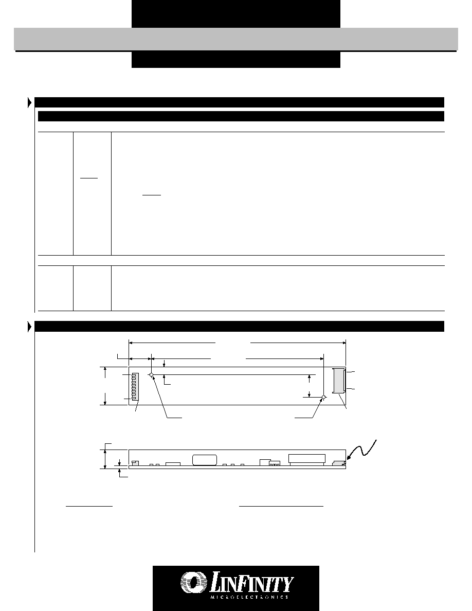
M E C H A N I C A L O U T L I N E
4.79 (121.6)
3.88 (98.55)
.40
(10.16)
.160 (4.06)
.400 (10.16)
0.125 (3.18) Diameter Hole, 2 places
No other holes on board.
.72
(18.29)
2-2
2-1
Connector CN-2
Connector CN-1
1-1
1-8
.031 (0.8)
All dimensions in inches (mm)
.315 Max. (8)
Warning!!
High Voltage
Present
Connectors:
Recommended Mate:
CN-1
= MOLEX 53261-0890
Pins: 50079-8100*, Housing: 51021-0800
*
Loose (-8000, Chain) Recommended #26 AWG wiring
CN-2
= JST SM02(8.0) B-BHS-TB
Pins: 5BH-001T-P0.5, Housing: BHR-03VS-1
Note: All samples are equipped with connector mates and cable.
5 V C C F L I
N V E R T E R
M
O D U L E S
LXM1597-01
P R O D U C T D A T A B O O K 1 9 9 6 / 1 9 9 7
Copyright © 1998
Rev. 0.6a 10/00
4
Not Recommended for New Designs
P
A T E N T
P
E N D I N G
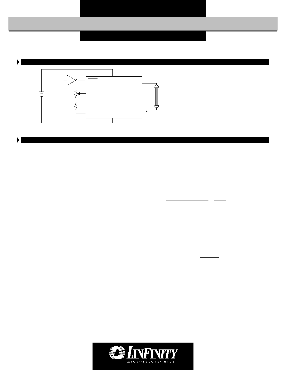
C O N N E C T I O N D I A G R A M
R
1
= 100k typical, 5k minimum
R
2
= Value optional to determine lowest
brightness setting
R
2
= 0.5 R
1
minimum
Lamp Current (%) =
x 100
V
BRITE
V
REF
FIGURE 1 -- Recommended Connection Diagram
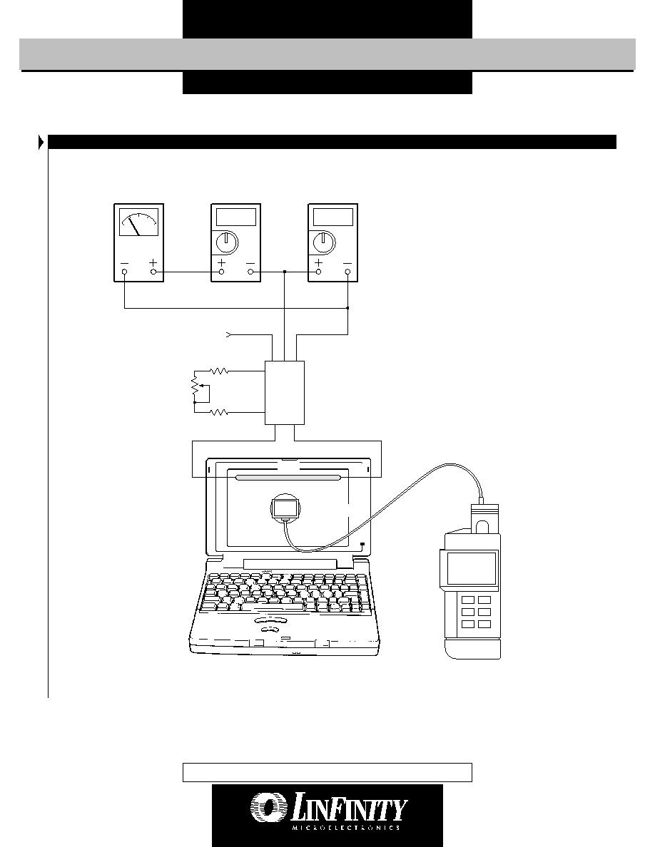
E F F I C I E N C Y M E A S U R E M E N T S E T U P
INTRODUCTION
The best method for evaluating high voltage, high frequency
inverters is by directly measuring light output versus power
input. This method is highly recommended when evaluating
inverter modules.
The following sections outline the recommended method
for testing these modules.
the end of the 30 minute period read the light output in cd/m
2
(1 cd/m
2
= 1 Nit), as well as input voltage and current. Typical
applications require about 70 to 100 Nits out of the screen.
With the temperature probe record the temperature rises of
critical components such as the high voltage transformer and
the inductor.
The light output efficiency of the module can be calculated
by the following equation:
Eff =
=
For competitive evaluation with another module from Linfinity
or another manufacturer repeat the above steps for the second
module.
After taking the data on the second module, compare the
temperature rises on the transformer and inductors. The main
figure of merit comparison is done between the two Eff num-
bers as follows:
Percent More Efficient =
* 100
The result of the above shows how much more efficient mod-
ule #1 is than module #2.
Light Output (in Nits)
V
IN (DC)
* I
IN (DC)
Nits
Watt
Eff
1
- Eff
2
Eff
2
EQUIPMENT REQUIRED
1) Two DVM's with 0.1% or better accuracy.
2) A lab power supply. (0 - 20V, 0 - 2A)
3) The target notebook or LCD panel.
4) A Tektronix J1803 Luminance Head.
5) A Tektronix J17 Luminance Color Photometer.
6) A non-contact infrared temperature sensor
(i.e. Fluke 80T-IR) with a mV meter.
MEASUREMENT SETUP
Figure 2 shows the connection diagram for light output mea-
surements. The photometer luminance head (J1803) is posi-
tioned directly in the center of the LCD screen. For best re-
sults open an application such as the Paintbrush program and
choose the maximized view so that the entire screen is "white".
After application of the power to the CCFL wait at least 30
minutes to allow for the lamp and light output to stabilize. At
LXM1597-01
V
REF
BRITE
AGND
From Power
Management
Logic
LAMP HI
V
IN
SLEEP
LAMP LO
GND
R
1
100k
R
2
51k
CMOS or TTL gate
CFL
TUBE
Longest Lead
5 V C C F L I
N V E R T E R
M
O D U L E S
LXM1597-01
P R O D U C T D A T A B O O K 1 9 9 6 / 1 9 9 7
5
Copyright © 1998
Rev. 0.6a 10/00
Not Recommended for New Designs
P
A T E N T
P
E N D I N G
E F F I C I E N C Y M E A S U R E M E N T S E T U P
(continued)
DC
Power Supply
DC
Amp Meter
DC
Volt Meter
Inverter
Module
Sleep Control = Logic "1"
Dimming
Control
CCFL
J17
Photometer
P
IN
= V
DC *
I
DC
J1803
Luminance
Head
FIGURE 2 -- Light Output Measurement Setup
PRELIMINARY DATA - Information contained in this document is pre-production data, and is proprietary to LinFinity. It may
not modified in any way without the express written consent of LinFinity. Product referred to herein is offered in sample form
only, and Linfinity reserves the right to change or discontinue this proposed product at any time.