Microsemi
Scottsdale Division
8700 E. Thomas Rd. PO Box 1390, Scottsdale, AZ 85252 USA, (480) 941-6300, Fax: (480) 947-1503
Page 1
Copyright
©
2001
MSCXXXX.PDF 6-03 2002 REV 0
WWW.
Microsemi
.
COM
SRLC05
Low Capacitance TVSarray TM
S C O T T S D A L E
D I V I S I O N
SRLC05
DESCRIPTION
This TRANSIENT VOLTAGE SUPPRESSOR (TVS) is packaged in an
SOT-143 configuration with very low capacitance giving protection for two high
speed data lines connected to terminals 2 and 3. This protection is from
electrostatic discharge (ESD) and other induced voltage surges such as electrical
fast transient/burst (EFT) that can damage or upset sensitive circuitry as defined in
IEC 61000≠4-2 and IEC 61000-4-4. With its four steering diodes and one TVS,
any positive voltage on the data lines exceeding one diode voltage drop above the
positive voltage supply line (Vcc) connected to terminal 4 will be diverted away
from the protected line to the supply line. If this also exceeds the TVS voltage, the
surge is directed to ground (Gnd) at terminal 1. Negative voltages greater than one
voltage drop are diverted to ground. This SRLC05 can also serve as a bi-
directional, low capacitance TVS when simply using terminals 2 and 3. In a similar
configuration, the terminal 1 can optionally be tied to ground.
IMPORTANT:
For the most current data, consult
MICROSEMI
's website: http://www.microsemi.com
ELECTRICAL CHARACTERISTICS PER LINE @ 25∞C Unless otherwise specified
BREAKDOWN
VOLTAGE
V
BR
@1 mA
VOLTS
CLAMPING
VOLTAGE
V
C
@ 1 Amp
(Figure 2)
VOLTS
CLAMPING
VOLTAGE
V
C
@ 5 Amp
(Figure 2)
VOLTS
PEAK FORWARD
VOLTAGE
V
f
@ 1 Amp
(Figure 2)
VOLTS
STANDBY
CURRENT
I
D
@ 5 Volts
µA
CAPACITANCE
C
@0V ,(f = 1 MHz)
Between I/O pins
and GND
pF
CAPACITANCE
C
@0V ,(f = 1MHz)
Between I/O pins
pF
PART
NUMBER
DEVICE
MARKING
MIN
MAX
MAX
MAX
MAX
TYP
MAX
TYP
MAX
SRLC05
R05
5.6
8
11
2
2
4
6
2
3
Note: Transient Voltage Suppressor (TVS) product is normally selected based on its stand off voltage V
WM
. Product selected
voltage should be equal to or greater than the continuous peak operating voltage of the circuit to be protected.
T V S array
TM
S E R I E S
APPLICATIONS
∑
EIA-RS485 data rates:
5 Mbs
∑
10 Base T Ethernet
∑
USB date rate: 900 Mbs
∑
Video line protection
∑
Wan/Lan
∑
ISDN S/T
F E A T U R E S
∑
Protects 2 high-speed data lines
∑
Surge protection per IEC 61000-4-2, IEC 61000-4-4
∑
Optionally provides bi-directional protection
∑
ULTRA LOW CAPACITANCE 6 pF
∑
UL94V-0 Flammability Classification
M A X I M U M R A T I N G S
∑
Operating Temperature: -55∞C to +150∞C
∑
Storage Temperature: -55∞C to +150∞C
∑
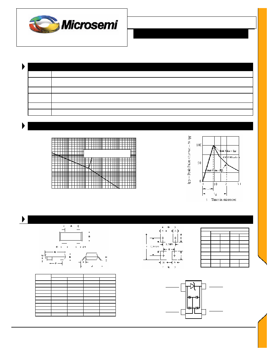
Peak Pulse Power: 200 watts (8/20 µs, Figure 1)
∑
Pulse Repetition Rate: < .01%
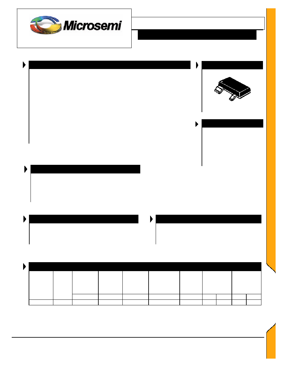
M E C H A N I C A L
∑
Molded SOT-143 Surface Mount
∑
Weight: 0.035 grams (approximate)
∑
Body marked with device marking code
∑
Pin #1 defined by dot on top of package
Microsemi
Scottsdale Division
8700 E. Thomas Rd. PO Box 1390, Scottsdale, AZ 85252 USA, (480) 941-6300, Fax: (480) 947-1503
Page 2
Copyright
©
2001
MSCXXXX.PDF 6-03 2002 REV 0
WWW.
Microsemi
.
COM
SRLC05
Low Capacitance TVSarray TM
S C O T T S D A L E
D I V I S I O N
Figure 1
SRLC05
INCHES
MILLIMETERS
DIM
MIN
MAX
MIN
MAX
A
0.070
0.080
1.78
2.03
B
0.047
0.055
1.20
1.40
C
0.030
0.037
0.77
0.94
C1
0.015
0.020
0.37
0.50
D
0.110
0.119
2.80
3.04
E
0.035
0.044
0.89
1.17
F
0.071
0.079
1.80
2.00
G
0.0006
0.006
0.013
0.05
H
0.003
0.007
0.085
0.17
I
0.018
0.023
0.45
0.60
J
0.083
0.093
2.10
2.50
S Y M B O L S & D E F I N I T I O NS
Symbol
DEFINITION
V
WM
Stand Off Voltage: Maximum dc voltage that can be applied over the operating temperature range.
Vwm must be selected to be equal or be greater than the operating voltage of the line to be protected.
V
BR
Minimum Breakdown Voltage: The minimum voltage the device will exhibit at a specified current
V
C
Clamping Voltage: Maximum clamping voltage across the TVS device when subjected to a given current at a
pulse time of 20
µ
s.
I
D
Standby Current: Leakage current at V
WM.
C
Capacitance: Capacitance of the TVS as defined @ 0 volts at a frequency of 1 MHz and stated in picofarads.
G R A P H S
O U T L I N E A N D S C H E M A T I C
Figure 2
Pulse Wave Form
DIMENSIONS
INCHES
MM
DIM
MIN
MAX
MIN
MAX
A
.032
.040
0.80
1.00
A1
.040
.048
1.00
1.20
B
---
.057
---
1.44
C
---
.087
---
2.20
D
.075 BSC
1.90 BSC
E
.067 BSC
1.70 BSC
G
.032
.040
0.80
1.00
H
.134
.140
3.40
3.60
PAD LAYOUT
SCHEMATIC
OUTLINE
4
3
1
2
100 nS
1µS
10µS
1mS
10mS
100Ms
t
d
≠ PULSE TIME - SEC
P
P
≠
PEAK
PULSE
POWER
-
KW
10000
1000
100
10
8/20µs 200W Pulse
Gnd
Signal Line
Signal Line
+V or Vcc