 | –≠–ª–µ–∫—Ç—Ä–æ–Ω–Ω—ã–π –∫–æ–º–ø–æ–Ω–µ–Ω—Ç: UC2844AD | –°–∫–∞—á–∞—Ç—å:  PDF PDF  ZIP ZIP |
D E S C R I P T I O N
K E Y F E A T U R E S
s
s
s
s
s LOW START-UP CURRENT. (0.5mA max.)
s
s
s
s
s TRIMMED OSCILLATOR DISCHARGE
CURRENT.
(See Product Highlight)
p OPTIMIZED FOR OFF-LINE AND DC-TO-DC
CONVERTERS.
p AUTOMATIC FEED FORWARD
COMPENSATION.
p PULSE-BY-PULSE CURRENT LIMITING.
p ENHANCED LOAD RESPONSE
CHARACTERISTICS.
p UNDER-VOLTAGE LOCKOUT WITH
HYSTERESIS.
p DOUBLE PULSE SUPPRESSION.
p HIGH-CURRENT TOTEM POLE OUTPUT.
p INTERNALLY TRIMMED BANDGAP
REFERENCE.
p 500KHz OPERATION.
p LOW R
O
ERROR AMPLIFIER.
The UC184xA family of control ICs
provides all the necessary features to
implement off-line fixed-frequency,
current-mode switching power supplies
with a minimum of external compo-
nents. The current mode architecture
demonstrates improved load regulation,
pulse-by-pulse current limiting and
inherent protection of the power supply
output switch. The IC includes: A
bandgap reference trimmed to ±1%
accuracy, an error amplifier, a current
sense comparator with internal clamp to
1V, a high current totem pole output
stage for fast switching of power
MOSFET's, and an externally program-
mable oscillator to set frequency and
maximum duty cycle. The under-
voltage lock-out is designed to operate
with 250µA typ. start-up current,
allowing an efficient bootstrap supply
voltage design. Available options for
this family of products, such as start-up
voltage hysteresis and duty cycle, are
summarized below in the Available
Options section. The UC184xA family
of control ICs is also available in 14-pin
SOIC package which makes the Power
Output Stage Collector and Ground pins
available.
A P P L I C A T I O N S
s
s
s
s
s ECONOMICAL OFF-LINE FLYBACK OR
FORWARD CONVERTERS.
s DC-DC BUCK OR BOOST CONVERTERS.
s LOW COST DC MOTOR CONTROL.
A
V A I L A B L E
O
P T I O N S
Part #
Start-Up Hysteresis Max. Duty
Voltage
Cycle
P A C K A G E O R D E R I N F O R M A T I O N
T
A
(∞C)
Plastic DIP
8-pin
0 to 70
UC384xAM
UC384xADM
UC384xAD
--
-40 to 85
UC284xAM
UC284xADM
UC284xAD
UC284xAY
-55 to 125
--
--
--
UC184xAY
M
Plastic SOIC
8-pin
DM
Plastic SOIC
14-pin
D
Ceramic DIP
8-pin
Y
Note: All surface-mount packages are available in Tape & Reel. Append the letter "T" to part number. (i.e. UC3842ADMT)
UCx842A
16V
6V
<100%
UCx843A
8.4V
0.8V
<100%
UCx844A
16V
6V
<50%
UCx845A
8.4V
0.8V
<50%
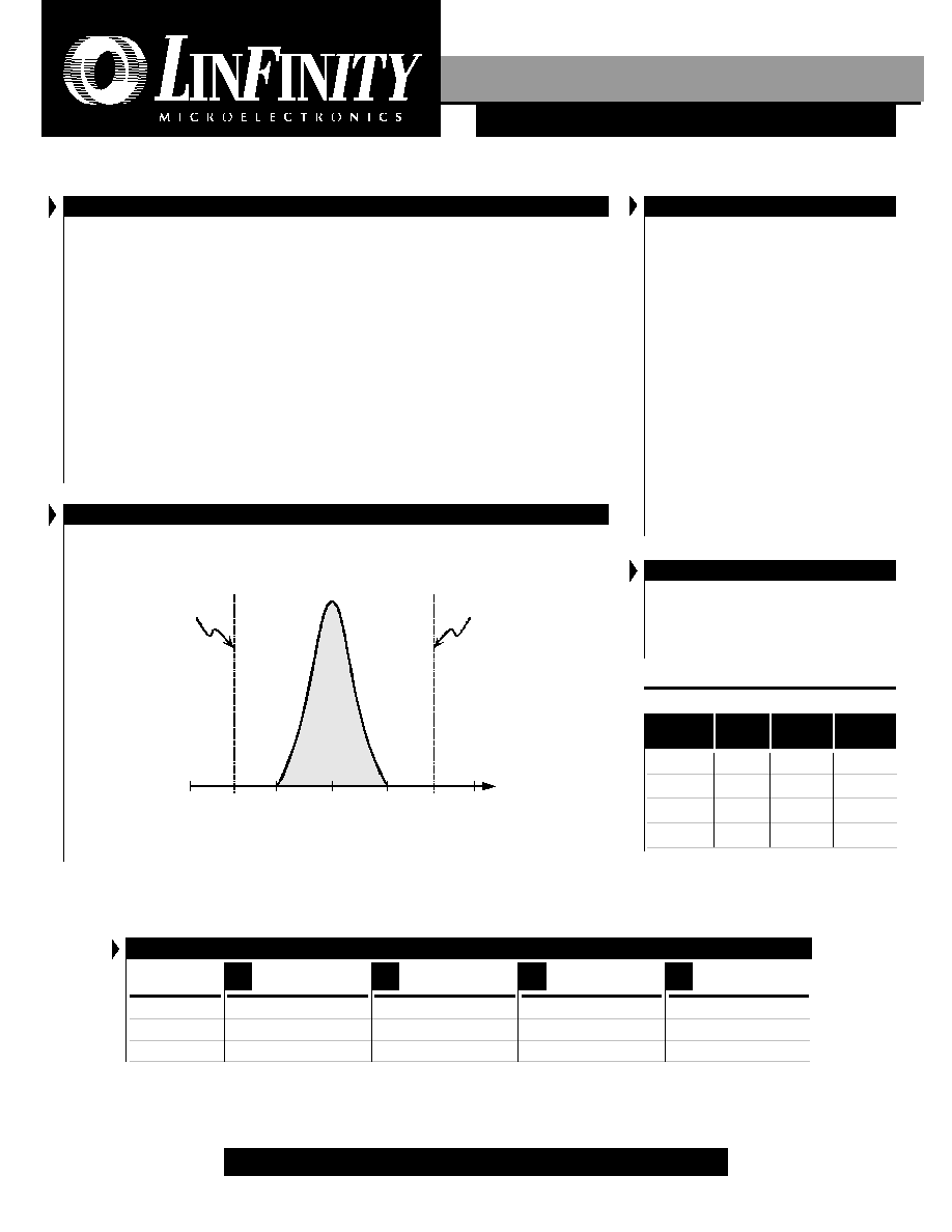
P R O D U C T H I G H L I G H T
C
OMPARISON
OF
UC384
X
A
VS
. SG384
X
D
ISCHARGE
C
URRENT
UC384xA
7.5
8.3
9.3
Mean
SG384x
Min. Limit
7.8
-3
8.8
+3
SG384x
Max. Limit
Discharge Current Distribution - mA
T
A
=25∞C
C
U R R E N T
M
O D E
P W M C
O N T R O L L E R
P
R O D U C T I O N
D
A T A
S
H E E T
T
H E
I
N F I N I T E
P
O W E R
O F
I
N N O V A T I O N
Copyright © 1995
Rev. 1.2 12/95
F O R F U R T H E R I N F O R M A T I O N C A L L ( 7 1 4 ) 8 9 8 - 8 1 2 1
11861 W
ESTERN
A
VENUE
, G
ARDEN
G
ROVE
, CA. 92841
UC184xA/284xA/384xA
LIN D
O C
#: 1840
1
C
U R R E N T
M
O D E
P W M C
O N T R O L L E R
UC184xA/284xA/384xA
P R O D U C T D A T A B O O K 1 9 9 6 / 1 9 9 7
Copyright © 1995
Rev. 1.2 12/95
2
P
R O D U C T I O N
D
A T A
S
H E E T
ABSOLUTE MAXIMUM RATINGS
(Note 1)
Supply Voltage (Low Impedance Source) (V
CC
) ......................................................... 30V
Supply Voltage (I
CC
< 30mA) .......................................................................... Self Limiting
Output Current ............................................................................................................. ±1A
Output Energy (Capacitive Load) ................................................................................. 5µJ
Analog Inputs (V
FB
& I
SENSE
) ........................................................................ -0.3V to +6.3V
Error Amp Output Sink Current ............................................................................... 10mA
Power Dissipation at T
A
= 25∞C (M Package) .............................................................. 1W
Storage Temperature Range .................................................................... -65∞C to +150∞C
Lead Temperature (Soldering, 10 Seconds) ............................................................. 300∞C
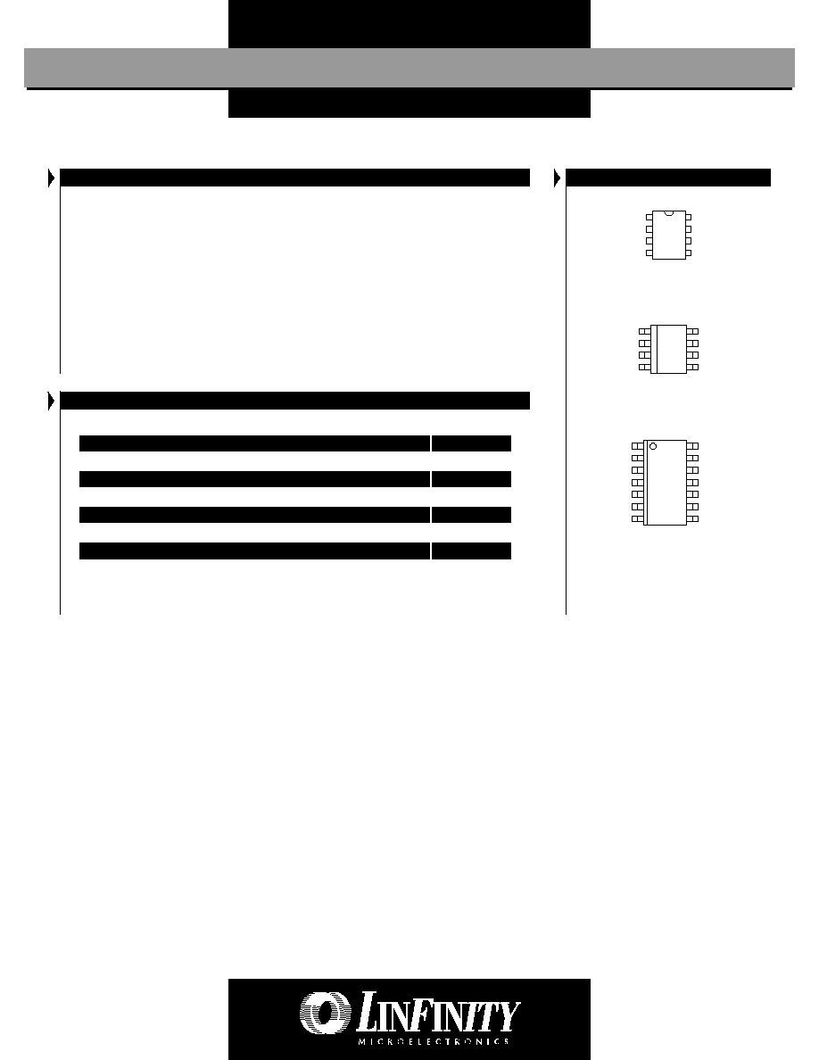
PACKAGE PIN OUTS
Note 1. Exceeding these ratings could cause damage to the device. All voltages are with respect
to Ground. Currents are positive into, negative out of the specified terminal. Pin
numbers refer to DIL packages only.
1
8
2
7
3
6
4
5
M & Y PACKAGE
(Top View)
M PACKAGE:
THERMAL RESISTANCE-JUNCTION TO AMBIENT,
JA
95∞C/W
DM PACKAGE:
THERMAL RESISTANCE-JUNCTION TO AMBIENT,
JA
165∞C/W
D PACKAGE:
THERMAL RESISTANCE-JUNCTION TO AMBIENT,
JA
120∞C/W
Y PACKAGE:
THERMAL RESISTANCE-JUNCTION TO AMBIENT,
JA
130∞C/W
Junction Temperature Calculation: T
J
= T
A
+ (P
D
x
JA
).
The
JA
numbers are guidelines for the thermal performance of the device/pc-board system.
All of the above assume no ambient airflow
THERMAL DATA
DM PACKAGE
(Top View)
V
REF
V
CC
OUTPUT
GND
COMP
V
FB
I
SENSE
R
T
/C
T
1
8
2
7
3
6
4
5
V
REF
N.C.
V
CC
V
C
OUTPUT
GND
PWR GND
COMP
N.C.
V
FB
N.C.
I
SENSE
N.C.
R
T
/C
T
1
14
2
13
3
12
4
11
5
10
6
9
7
8
D PACKAGE
(Top View)
COMP
V
FB
I
SENSE
R
T
/C
T
V
REF
V
CC
OUTPUT
GND
C
U R R E N T
M
O D E
P W M C
O N T R O L L E R
UC184xA/284xA/384xA
P R O D U C T D A T A B O O K 1 9 9 6 / 1 9 9 7
3
Copyright © 1995
Rev. 1.2 12/95
P
R O D U C T I O N
D
A T A
S
H E E T
E L E C T R I C A L C H A R A C T E R I S T I C S
(Unless otherwise specified, these specifications apply over the operating ambient temperatures for UC384xA with 0∞C
T
A
70∞C, UC284xA with -40∞C
T
A
85∞C,
UC184xA with -55∞C
T
A
125∞C; V
CC
=15V; R
T
=10K; C
T
=3.3nF. Low duty cycle pulse testing techniques are used which maintains junction and case temperatures equal
to the ambient temperature.)
Reference Section
Parameter
Symbol
Test Conditions
Output Voltage
V
REF
T
J
= 25∞C, I
L
= 1mA
Line Regulation
12
V
IN
25V
Load Regulation
1
I
O
20mA
Temperature Stability (Note 2 & 7)
Total Output Variation
Over Line, Load, and Temperature
Output Noise Voltage (Note 2)
V
N
10Hz
f
10kHz, T
J
= 25∞C
Long Term Stability (Note 2)
T
A
= 125∞C, t = 1000hrs
Output Short Circuit Current
I
SC
UC384xA
Units
Min. Typ. Max. Min. Typ. Max.
UC184xA/284xA
4.95 5.00 5.05 4.90 5.00 5.10
V
6
20
6
20
mV
6
25
6
25
mV
0.2
0.4
0.2
0.4
mV/∞C
4.9
5.1
4.82
5.18
V
50
50
µV
5
25
5
25
mV
-30
-100 -180
-30
-100 -180
mA
Oscillator Section
Initial Accuracy (Note 6)
T
J
= 25∞C
Voltage Stability
12
V
CC
25V
Temperature Stability (Note 2)
T
MIN
T
A
T
MAX
Amplitude (Note 2)
Discharge Current
T
J
= 25∞C, V
PIN 4
= 2V
V
PIN 4
= 2V, T
MIN
T
A
T
MAX
47
52
57
47
52
57
kHz
0.2
1
0.2
1
%
5
5
%
1.7
1.7
V
7.8
8.3
8.8
7.8
8.3
8.8
mA
7.5
8.8
7.6
8.8
mA
Output Low Level
V
OL
I
SINK
= 20mA
I
SINK
= 200mA
Output High Level
V
OH
I
SOURCE
= 20mA
I
SOURCE
= 200mA
Rise Time (Note 2)
T
R
T
J
= 25∞C, C
L
= 1nF
Fall Time (Note 2)
T
F
T
J
= 25∞C, C
L
= 1nF
UVLO Saturation
V
SAT
V
CC
= 5V, I
SINK
= 10mA
Current Sense Section
Gain (Note 3 & 4)
A
VOL
Maximum Input Signal (Note 3)
V
PIN 1
= 5V
Power Supply Rejection Ratio (Note 3)
PSRR
12
V
CC
25V
Input Bias Current
I
B
Delay to Output (Note 2)
T
pd
V
PIN 3
= 0 to 2V
Output Section
2.85
3
3.15 2.85
3
3.15
V/V
0.9
1
1.1
0.9
1
1.1
V
70
70
dB
-2
-10
-2
-10
µA
150
300
150
300
ns
0.1
0.4
0.1
0.4
V
1.5
2.2
1.5
2.2
V
13
13.5
13
13.5
V
12
13.5
12
13.5
V
50
150
50
150
ns
50
150
50
150
ns
0.7
1.2
0.7
1.2
V
( E l e c t r i c a l C h a r a c t e r i s t i c s c o n t i n u e n e x t p a g e . )
Error Amp Section
Input Voltage
V
PIN 1
= 2.5V
Input Bias Current
I
B
Open Loop Gain
A
VOL
2
V
O
4V
Unity Gain Bandwidth (Note 2)
UGBW
T
j
= 25∞C
Power Supply Rejection Ratio (Note 3)
PSRR
12
V
CC
25V
Output Sink Current
I
OL
V
PIN 2
= 2.7V, V
PIN 1
= 1.1V
Output Source Current
I
OH
V
PIN 2
= 2.3V, V
PIN 1
= 5V
Output Voltage High Level
V
OH
V
PIN 2
= 2.3V, R
L
= 15K to ground
Output Voltage Low Level
V
OL
V
PIN 2
= 2.7V, R
L
= 15K to V
REF
2.45 2.50 2.55 2.42 2.50 2.58
V
-0.3
-1
-0.3
-2
µA
65
90
65
90
dB
0.7
1
0.7
1
MHz
60
70
60
70
dB
2
6
2
6
mA
-0.5
-0.8
-0.5
-0.8
mA
5
6
5
6
V
0.7
1.1
0.7
1.1
V
C
U R R E N T
M
O D E
P W M C
O N T R O L L E R
UC184xA/284xA/384xA
P R O D U C T D A T A B O O K 1 9 9 6 / 1 9 9 7
Copyright © 1995
Rev. 1.2 12/95
4
P
R O D U C T I O N
D
A T A
S
H E E T
E L E C T R I C A L C H A R A C T E R I S T I C S
(Con't.)
Under-Voltage Lockout Section
Parameter
Symbol
Test Conditions
Start Threshold
x842A/4A
x843A/5A
Min. Operation Voltage After Turn-On
x842A/4A
x843A/5A
UC384xA
Units
Min. Typ. Max. Min. Typ. Max.
UC184xA/284xA
15
16
17
14.5
16
17.5
V
7.8
8.4
9.0
7.8
8.4
9.0
V
9
10
11
8.5
10
11.5
V
7.0
7.6
8.2
7.0
7.6
8.2
V
PWM Section
Maximum Duty Cycle
x842A/3A
x844A/5A
Minimum Duty Cycle
94
96
100
94
96
100
%
47
48
50
47
48
50
%
0
0
%
Total Standby Section
Start-Up Current
Operating Supply Current
I
CC
Zener Voltage
V
Z
I
CC
= 25mA
0.3
0.5
0.3
0.5
mA
11
17
11
17
mA
30
35
30
35
V
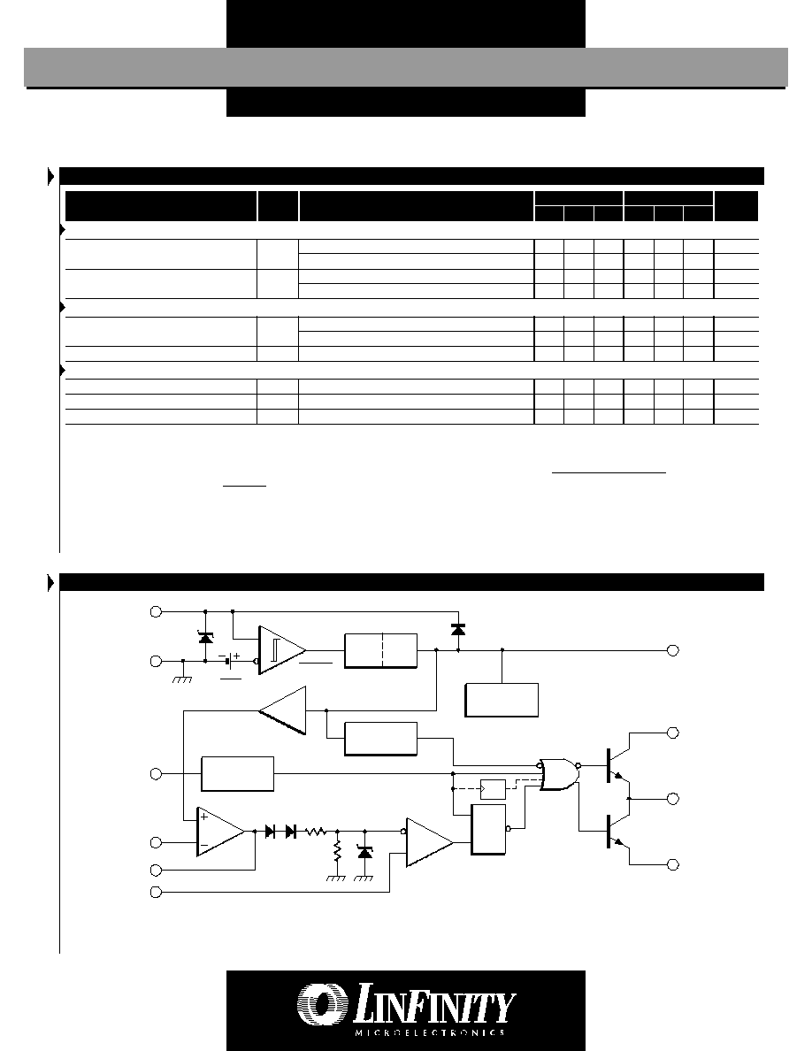
B L O C K D I A G R A M
* - V
CC
and V
C
are internally connected for 8 pin packages.
** - POWER GROUND and GROUND are internally connected for 8 pin packages.
*** - Toggle flip flop used only in x844A and x845A series.
Notes: 2. These parameters, although guaranteed, are not 100% tested in
production.
3. Parameter measured at trip point of latch with V
VFB
= 0.
4. Gain defined as: A
VOL
=
; 0
V
ISENSE
0.8V.
5. Adjust V
CC
above the start threshold before setting at 15V.
6. Output frequency equals oscillator frequency for the UC1842A
and UC1843A. Output frequency is one half oscillator frequency
for the UC1844A and UC1845A.
7. "Temperature stability, sometimes referred to as average temperature
coefficient, is described by the equation:
Temp Stability =
V
REF
(max.) & V
REF
(min.) are the maximum & minimum reference
voltage measured over the appropriate temperature range. Note that
the extremes in voltage do not necessarily occur at the extremes in
temperature."
V
REF
(max.) - V
REF
(min.)
T
J
(max.) - T
J
(min.)
V
COMP
V
ISENSE
UVLO
S / R
5V
Ref
Internal
Bias
34V
Error Amp
1V
Current Sense
Comparator
PWM
Latch
S
R
R
Oscillator
2R
**
T
***
V
REF
Good Logic
2.5V
UVLO
16V (1842A/4A)
8.4V (1843A/5A)
Hysteresis
6V (1842A/4A)
0.8V (1843A/5A)
COMP
CURRENT SENSE
V
FB
R
T
/C
T
GROUND
*
V
CC
V
REF
5.0V
50mA
V
C
*
OUTPUT
POWER GROUND**
C
U R R E N T
M
O D E
P W M C
O N T R O L L E R
UC184xA/284xA/384xA
P R O D U C T D A T A B O O K 1 9 9 6 / 1 9 9 7
5
Copyright © 1995
Rev. 1.2 12/95
P
R O D U C T I O N
D
A T A
S
H E E T
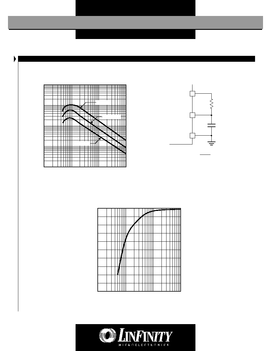
C H A R A C T E R I S T I C C U R V E S
FIGURE 1. -- OSCILLATOR FREQUENCY vs. TIMING
RESISTOR
300
3.0k
100k
0
100k
R
T
- (ohms)
Oscillator Frequency - (Hz)
10k
1M
1.0k
10.0k
30.0k
C
T
= 1nF
C
T
= 2.2nF
C
T
= 4.7nF
FIGURE 2. -- MAXIMUM DUTY CYCLE vs. TIMING RESISTOR
300
3.0k
100k
0
40.0
R
T
- (ohms)
Maximum Duty Cycle - (%)
20.0
60.0
1.0k
10.0k
30.0k
80.0
100.0
Note: Output drive frequency is half the oscillator frequency for
the UCx844A/5A devices.
8
4
5
V
REF
R
T
/C
T
GROUND
R
T
C
T
For R
T
> 5k, f
ª
1.72
R
T
C
T